 Many people remember this wonderful PC. I got this when I was 11. It took 28 years and now I decided to make expansion devices, which I really lacked then, as a hobby.
Idea
On the network, I saw several options for SD downloaders for such PCs, I didn’t like the presence of microcontrollers in them, I wanted to use “vintage, warm DIP” circuitry, which is why I decided to use “KR1533” on the domestic logic.As an add. RAM I applied UT62256. This is the only imported chip in the project. Of course, it was possible to install KP537RU10 or KP537RU25A, but firstly, they would have had to be installed not one but two (I planned 4 KB of additional RAM), and secondly I had UT62256, but I didn’t have KR537, and I didn’t have to order I wanted to. Therefore, I allowed myself the freedom to import, and then the idea came up to use all 32kB of additional RAM, with page switching. For the ROM I chose KR573RF5, there were just two clean ones.
Flow chart
After sitting over a cup of tea, I drew such a block diagram.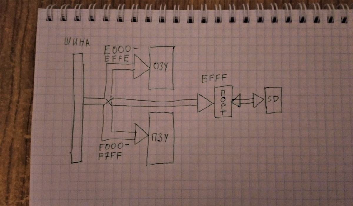 Here is the RAM chip, the ROM chip, and the PORT block. The PORT block has a parallel interface having 8 inputs and 8 outputs. When writing to the EFFF address, the written code is set at the outputs, and when reading from the same address, the read value corresponds to the status of the inputs. Three of the outputs and one of the inputs are connected to the SD card through a level converter.The RAM is represented by the UT62256 chip and has 32kB of memory. Since the range of E000-EFFE addresses is almost 4kB (4095 bytes), we get 8 pages that are selected by the PORT block, bits 1,2 and 3. That is, writing to the EFFF address sets the page in accordance with these three bits. Also reading from this port shows which page is currently selected (in the same bits). Total, we have 32760 bytes of additional RAM (4095x8str).The ROM chip is KR573RF5. It is connected to the address space F000-F7FF, and contains the BSVV code (BIOS), the task of this code is to initialize the SD card, load the OS from it and transfer control to it.Accordingly, after turning on the PC, we type in the GF000 System Monitor and press VK.In the future, there is an idea to modify the native ROM of the System Monitor to automatically boot the OS from the SD card, and the PC will go to the standard Monitor prompt if the download failed or was interrupted, for example, by pressing some key.I'll think about it again.
Scheme
About 2-3 hours at the computer, and I drew the following diagram in EAGLE.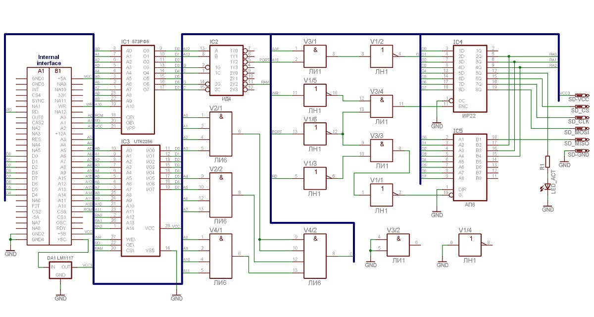 ZoomI drew based on the microcircuits that I had. It is possible that the number of logic chips can be reduced if other gates are used, but I only had one. And in the future, I will most likely optimize the circuit.Low level circuit parsing ...
... removed under the spoiler, I think few people are interested in this jungle.V3/1, A14 A15 , N3 , .1. V1/2 G, IC2. A B, A12 A13 . , , A14 A15, A12 A13. — 1110,
A15-1; A14-1; A13-1; A12-0. N2. , 5 11, - , , . 1 5, 2 11. , 1C , 2C , .1 5, .0 — 11.
: Exxx =1, «PORT», Exxx C=0, «RAM».
«C» , (A0-A11). xFFF, =1, =0. : «PORT» EFFF, «RAM» E000-EFFE.
«RAM» CS IC3, , , E000-EFFE . E000-EFFE . EFFF IC4, . «PORT» «WR» c V1/5, V1/6 V3/4.
EFFF IC5,
B0-B7.
. « » CS3 CS .
Layout assembly
Now I have no opportunity to poison the board at home, and I, taking a piece of foil-coated double-sided PCB, sawed out the necessary rectangle from it.This rectangle was firmly inserted into the PC “internal interface” slot, did not hang out and did not move. Next, I scratched the pads on the back and front. It turned out pretty well. Then the rough arrangement of microcircuits and the reconnaissance of holes. On the front side, I drilled it with a large drill so that the terminals of the microcircuits do not come in contact with the front foil. On the reverse side, I scratched the perimeter of each contact row and divided it into contact pads.The next step I put all the microcircuits (and the socket) and disappeared from the back. It took a lot of time the installation, which I conducted with a thin MGTF. He led the wiring on both sides, from the front he soldered directly to the legs of the microcircuits, from the back to the sites.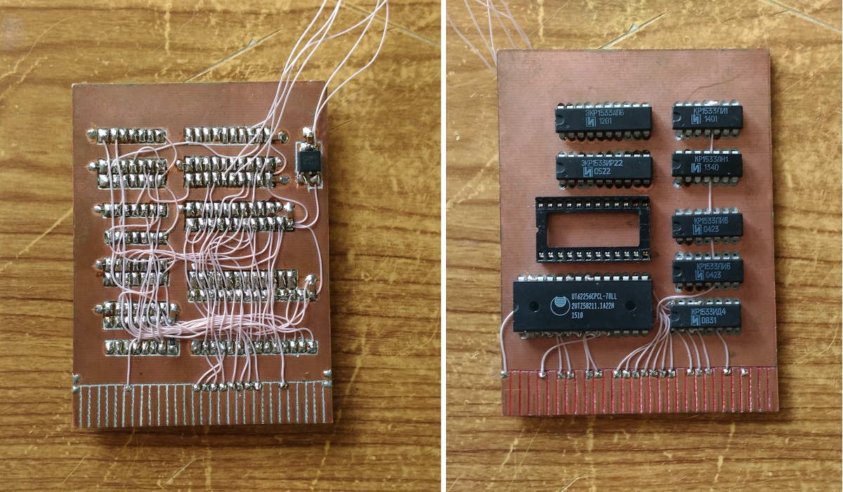 When the soldering process was over, I decided to pay attention to the signal level converter. The fact is that the SD card works with a voltage of 3.3V, and the chips KR1533AP6 and KR1533IR22 TTL 5v. Therefore, I had to make a small adapter scarf, on which the levels were limited to zener diodes.The signal coming from the SD card to the controller I just pulled to the source 3.3v. 10k resistor. As practice has shown, this signal does not need to be converted.
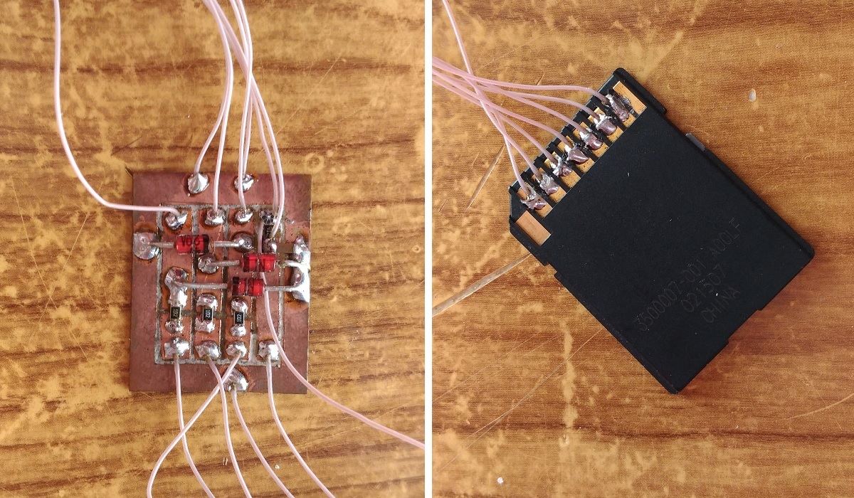 Although in the final version I will probably make a inverter based on a comparator.I used a microSD to SD adapter as a card holder.In general, there were no special problems in assembling the layout, although I was afraid that some of the microcircuits might be malfunctioning.
Layout Tests
First of all, I checked the RAM operation, wrote “AA”, “55”, “F0” and “0F” patterns to the E000-EFFE area using the System Monitor directive “F” and checked them using the “D” directive. Everything turned out to be normal.Then, with the “M” directive, I began to write different values to the EFFF address, and watch the changes on the legs of the register 153322 with a multimeter, the states corresponded to the recorded codes. Also, when reading from this port, the code contained the selected page, in accordance with the plan, and even when the MISO signal was closed to ground in the low bit, it turned out to be 0, and when opened 1.It was even somehow suspicious that all the microcircuits were working and the installation was successful no mistakes.BSVV
Of course, I didn’t have any special tools for writing programs for 58080. I had to write a program in a notebook (notepad), then translate it into codes manually.Created a file in the editor under DOS “HIEW” and began filling it with codes. For the basics, I took my project under AVR, in which there was standard initialization of the SD card. The project was old, and it did not use any file system, just a logger.First I wrote a low-level function of the SPI programming interface, and then a high-level SD card initialization routine.It turned out something like this algorithm ...... which is put under the spoiler, I think it is already known to everyone.1. () 90;
2. CS .1 10 FF;
3. CS .0;
4. CMD0;
5. 01, 7;
6. . =0, , 2;
7. CMD8;
8. ACMD41;
9. 00, 11
10. . =0, , 8;
11. CMD58.
12. 2 EFFE.
13. .
The OCR card register was also read in the initialization routine, and the 2nd byte in it was written to the EFFE address. This was necessary to determine the type of card.In the case of SDSC - 80h, and in the case of SDHC - C0h.If the initialization did not pass, then the message “SD CARD ERROR” was displayed and then the monitor went out without reset.I converted this BSVV into WAV and downloaded it to the PC via the tape input, then debugged it, corrected the source code and downloaded it again.Bridges
Now I have additional RAM, 32,760 bytes in size, divided into 8 pages. But how to navigate between pages? How can a program running on the first page invoke a routine located on the fourth?To solve this problem, I have provided software bridges. A bridge is a small area in ROM that mediates control transfer.For example, executing code must transfer control to page number 3, to address E4B5. Then, the executing code places the lower 12 bits (4B5) in the register pair of the processor HL, and in the upper four bits puts the value 3 - the page number. Now in the register pair HL the value 34B5 is written. And the code jumps (JMP) to the ROM area, which is called the JMP-Bridge, it's just going to a fixed address in the ROM. The code in this area extracts the page number from the high bits of the HL register pair and writes them to the register of the PORT block at the EFFF address. The third page of RAM is now displayed in the E000-EFFE area. The JMP-Bridge program resets the four high bits of the HL register pair and writes “E” there. Now in the HL register pair there is already a physical address E4B5, and here the JMP-Bridge program transfers control to it.This transfers control between pages.There is a CALL-Bridge, it is needed to call a subroutine with a return, and differs from JMP-Bridge by saving the current page on the stack, and the reverse procedure for returning.The next two bridges are STA-Bridge and LDA-Bridge. As the names suggest, the first one writes the Battery register to a logical address (in HL), and the second one reads data from the logical address into this register.Thanks to these two bridges, a program executing from one page can store data in another.OS loading
If you look at the boot sector of the SD card, you can see that the text “Disk error, press any key to restart” is located at addresses 1AC-1D4.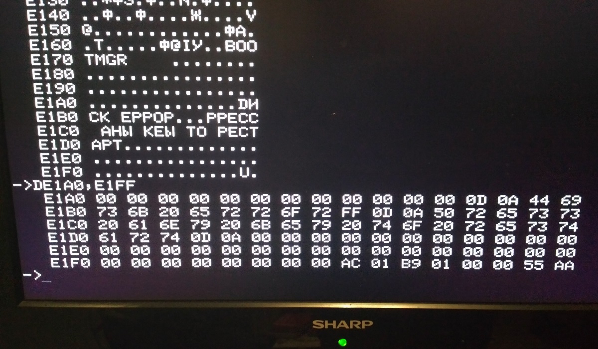 Yes, it’s so strange how it looks in the photo, because the character encoding of Mikroshi does not coincide with ASCII.I decided to use this area to place the data there for downloading the PC.First of all, I put the code 00 in position 1BA, and thereby cut the record. Now, just “Disk error” should be displayed and that’s it. The remaining bytes are mine. The principle is simple, 6 bytes MicrOS signature, and 4 bytes address on the SD card of the beginning of the file with OS. In BSVV, I wrote down, after receiving the boot sector from the SD card, the signature is checked, and if it is, then take the next 4 bytes and use it as the sector address for loading the OS.If there is no signature, the message “OS DOWNLOAD ERROR” is displayed and the System Monitor goes out without reset.
Total
And now, finally, everything works. BSVV is written, but I still need to write it to ROM.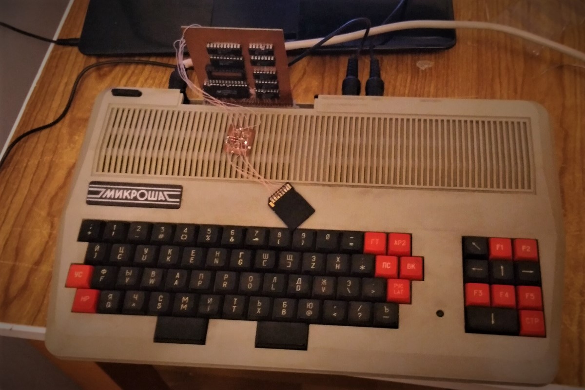 And for this, I need to edit all the addresses of subroutine calls and jumps, since this processor has absolute addressing. And I wrote BSVV for the region 6000-67FF to load in RAM. But now we need to change all 6xxx to Fxxx.In addition, I am in the “popanetsky” conditions. I have a ROM programmer, but it's an old one, under an LPT port. And there is not a single computer with LPT. But there is a pair of Atmega32A, in the PDIP40 package and a breadboard. You may need to emulate LPT using AVR. But maybe it will all work out ...That's all for now. Thank you for the attention! To be continued…