We continue to move towards the creation of real devices based on the Redd FPGA complex. For another All-Hardware project, I need a simple logic analyzer, so we will move in this direction. Lucky - and get to the USB bus analyzer (but this is still in the long run). The heart of any analyzer is RAM and a unit that first uploads data to it and then retrieves it. Today we will design it.To do this, we will master the DMA block. In general, DMA is my favorite topic. I even did a great article about DMA on some ARM controllers . From that article it is clear that DMA takes clock cycles from the bus. In the current article, we will consider how things are going with the FPGA-based processor system.
Hardware Creation
We begin to create the hardware. In order to understand how much the DMA block conflicts with clock cycles, we will need to take accurate measurements at high load on the Avalon-MM bus (Avalon Memory-Mapped). We have already found out that the Altera JTAG-to-Avalon-MM bridge cannot provide high bus loads. Therefore, today we have to add a processor core to the system so that it accesses the bus at high speed. How this is done has been described here . For the sake of optimality, let's disable both caches for the processor core, but create one strongly connected bus, as we did here .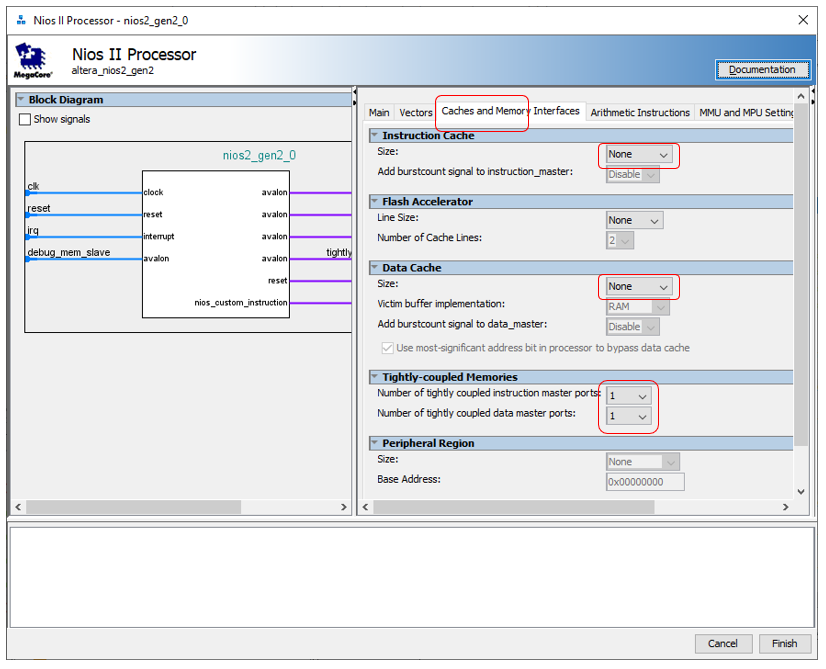 Add 8 kilobytes of program memory and data memory. Remember that the memory must be dual-port and have an address in a special range (to prevent it from jumping, lock it, we discussed the reasons for this here ).
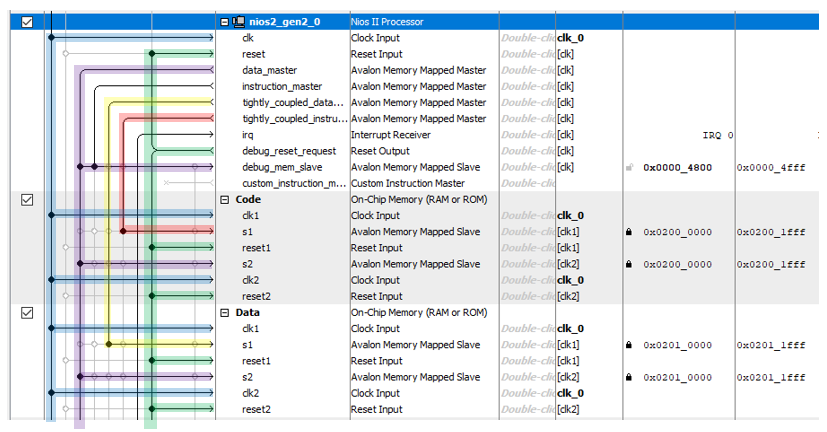 We have already created the project a thousand times, so there is nothing particularly interesting in the creation process itself (if anything, all the steps for creating it are described here ).The base is ready. Now we need a data source that we will put in memory. The ideal thing is a constantly ticking timer. If during some measure the DMA block was not able to process the data, then we will immediately see this by the missing value. Well, that is, if in memory there are values 1234 and 1236, it means that on the clock, when the timer issued 1235, the DMA block did not transfer data. Create a fileTimer_ST.sv with such a simple counter:
module Timer_ST (
  input              clk,
  input              reset,

  input  logic       source_ready,
  output logic       source_valid,
  output logic[31:0] source_data

);
    logic [31:0] counter;
    always @ (posedge clk, posedge reset)
    if (reset == 1)
    begin
        counter <= 0;
    end else
    begin
        counter <= counter + 1;
    end

    assign source_valid = 1;
    assign source_data [31:24] = counter [7:0];
    assign source_data [23:16] = counter [15:8];
    assign source_data [15:8] = counter [23:16];
    assign source_data [7:0] = counter [31:24];

endmodule
This counter is like a pioneer: it is always ready (at the output source_valid is always one) and it always counts (except for the moments of the reset state). Why the module has exactly these signals - we discussed in this article .Now we create our own component (how this is done is described here ). Automation mistakenly chose the Avalon_MM bus for us. Replace it with avalon_streaming_source and map the signals as shown below: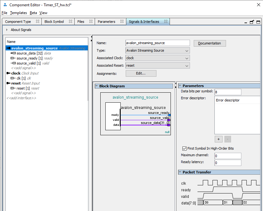 Great. Add our component to the system. Now we are looking for the DMA block ... And we find not one, but three. All of them are described in the document Embedded Peripheral IP User Guide from Altera (as always, I give names, but not links, since links always change).
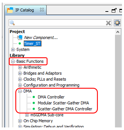 Which one to use? I can not resist nostalgia. Back in 2012, I made a system based on the PCIe bus. All manuals from Altera contained an example based on the first of these blocks. But he with the PCIe component gave a speed of no more than 4 megabytes per second. In those days, I spat and wrote my DMA block. Now I don’t remember his speed, but he drove the data from SATA drives to the limit of the capabilities of drives and SSDs of those times. That is, I have sharpened a tooth on this block. But I will not slip into a comparison of the three blocks. The fact is that today we have to work with a source based on Avalon-ST (Avalon Streaming Interface), and only Modular Scatter-Gather DMA block supports such sources . Here we put it on the diagram.In the block settings, select the modeStreaming to Memory Mapped . Plus - I want to drive data from launch to filling SDRAM, so I replaced the maximum data transfer unit from 1 kilobyte to 4 megabytes. True, I was warned that in the end, the FMax parameter will not be so hot (even if you replace the maximum block with 2 kilobytes). But for today, FMax is acceptable (104 MHz), and then we'll figure it out. I left the remaining parameters unchanged. You can also set the transmission mode to Full Word Access Only, this will increase FMax to 109 MHz. But we will not fight for performance today.
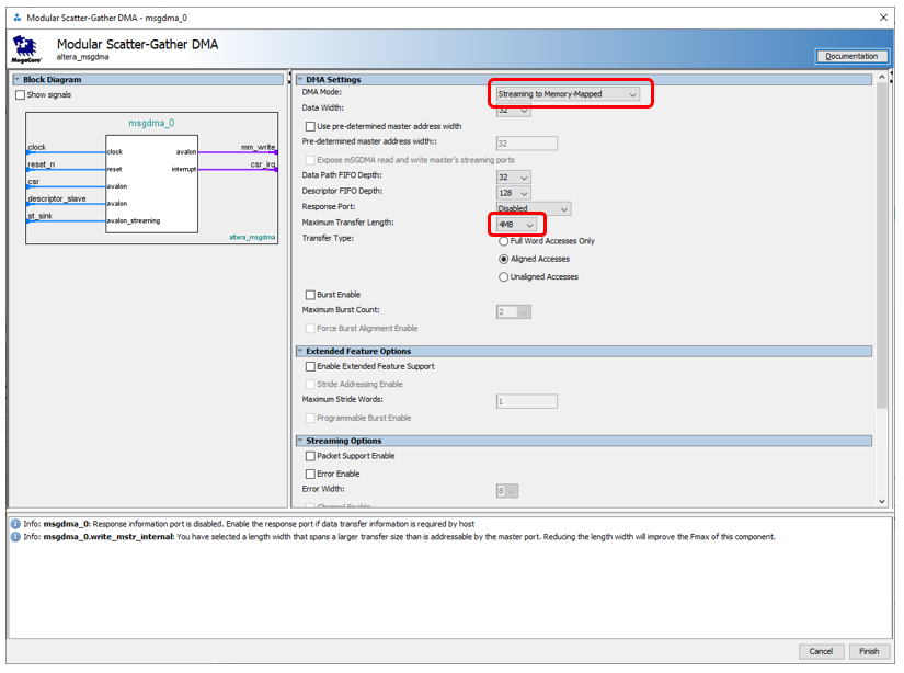 So. The source is, DMA is. Receiver ... SDRAM? In future combat conditions, yes. But today we need a memory with known characteristics. Unfortunately, SDRAM needs to periodically send commands that take several clock cycles, plus this memory can be occupied by regeneration. Therefore, instead of it, we will now use the built-in FPGA memory. Everything is working for her in one step, without unpredictable delays.Since the SDRAM controller is single-port, the built-in memory can also be used exclusively in single-port mode. It is important. The fact is that we want to write to the memory using the DMA block master, but on the other hand, we want to read from this memory using the processor core or the Altera JTAG-to-Avalon-MM block. The hand reaches out and connect the write and read blocks to two different ports ... But you can’t! Rather, it is forbidden by the conditions of the problem. Because today it is possible, but tomorrow we will replace the memory with an exclusively single-port one. In general, we get such a block of three components (timer, DMA and memory):
 Well, and just for the sake of proforma, I’ll add UT and sysid to the JTAG system (although the second one didn’t help, I still had to conjure it with a JTAG adapter). What it is, and how their addition solves small problems, we have already studied. I will not tint the tires, everything is clear with them. Just show how it all looks in my project:
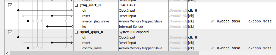 That's it. The system is ready. We assign addresses, assign processor vectors, generate a system (do not forget that you need to save with the same name as the project itself, then it will go to the top level of the hierarchy), add it to the project. Make the reset leg virtual, connect clk to pin_25 leg. We are assembling the project, pouring it into the equipment ... How is it, poor thing, in the empty office because of the total remote location? .. It’s lonely and scary for her, probably, alone ... But I was distracted.
Creating a software part
Training
In the BSP Editor with the usual movement of the hand I turn on C ++ support. I so often inserted a screenshot of this case that I stop doing it. But another screenshot, although it has already been seen, is still so common. So let's discuss it one more time. We remember that the system is trying to put data in the largest piece of memory. And such is Buffer . Therefore, we force everything to Data :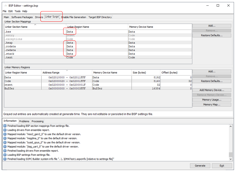
Program experiment
We make a code that simply fills the memory with the contents of the source (in the role of the counter).View code#include "sys/alt_stdio.h"
#include <altera_msgdma.h>
#include <altera_msgdma_descriptor_regs.h>
#include <system.h>
#include <string.h>
int main()
{
alt_putstr("Hello from Nios II!\n");
memset (BUFFER_BASE,0,BUFFER_SIZE_VALUE);
// ,
IOWR_ALTERA_MSGDMA_CSR_CONTROL(MSGDMA_0_CSR_BASE,
ALTERA_MSGDMA_CSR_STOP_DESCRIPTORS_MASK);
// , ,
// , . .
// FIFO
IOWR_ALTERA_MSGDMA_DESCRIPTOR_READ_ADDRESS(MSGDMA_0_DESCRIPTOR_SLAVE_BASE,
(alt_u32)0);
IOWR_ALTERA_MSGDMA_DESCRIPTOR_WRITE_ADDRESS(MSGDMA_0_DESCRIPTOR_SLAVE_BASE,
(alt_u32)BUFFER_BASE);
IOWR_ALTERA_MSGDMA_DESCRIPTOR_LENGTH(MSGDMA_0_DESCRIPTOR_SLAVE_BASE,
BUFFER_SIZE_VALUE);
IOWR_ALTERA_MSGDMA_DESCRIPTOR_CONTROL_STANDARD(MSGDMA_0_DESCRIPTOR_SLAVE_BASE,
ALTERA_MSGDMA_DESCRIPTOR_CONTROL_GO_MASK);
// ,
IOWR_ALTERA_MSGDMA_CSR_CONTROL(MSGDMA_0_CSR_BASE,
ALTERA_MSGDMA_CSR_STOP_ON_ERROR_MASK
& (~ALTERA_MSGDMA_CSR_STOP_DESCRIPTORS_MASK)
&(~ALTERA_MSGDMA_CSR_GLOBAL_INTERRUPT_MASK)) ;
//
static const alt_u32 errMask = ALTERA_MSGDMA_CSR_STOPPED_ON_ERROR_MASK |
ALTERA_MSGDMA_CSR_STOPPED_ON_EARLY_TERMINATION_MASK |
ALTERA_MSGDMA_CSR_STOP_STATE_MASK |
ALTERA_MSGDMA_CSR_RESET_STATE_MASK;
volatile alt_u32 status;
do
{
status = IORD_ALTERA_MSGDMA_CSR_STATUS(MSGDMA_0_CSR_BASE);
} while (!(status & errMask) &&(status & ALTERA_MSGDMA_CSR_BUSY_MASK));
alt_putstr("You can play with memory!\n");
/* Event loop never exits. */
while (1);
return 0;
}
We start, we wait for the message "You can play with memory!" , put the program on pause and look at the memory, starting from address 0. At first I was very scared: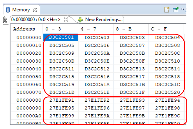 From address 0x80, the counter changes its value sharply. Moreover, a very large amount. But it turned out that everything is fine. At our place, the counter never stops and is always ready, and DMA has its own read-ahead queue. Let me remind you the settings of the DMA block:
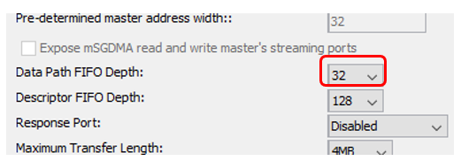 0x80 bytes are 0x20 thirty-two-bit words. Just 32 decimal. It all fits together. In debugging conditions, this is not scary. In combat conditions, the source will work more correctly (its readiness will be reset). Therefore, we simply ignore this section. In other areas, the meter counts sequentially. I will show only the dump fragment in width. Take a word that I examined it in its entirety.
 Not trusting my eyes, I wrote a code that automatically checks the data:
 volatile alt_u32* pData = (alt_u32*)BUFFER_BASE;
volatile alt_u32 cur = pData[0x10];
int nLine = 0;
for (volatile int i=0x11;i<BUFFER_SIZE_VALUE/4;i++)
{
if (pData[i]!=cur+1)
{
alt_printf("Problem at 0x%x\n",i*4);
if (nLine++ > 10)
{
break;
}
}
cur = pData[i];
}
He also does not reveal any problems.Trying to find at least some problems
In fact, the absence of problems is not always good. As part of the article, I needed to find the problems, and then show how they are fixed. After all, the problems are obvious. A busy bus cannot pass data without delays! There should be delays! But let's check why everything happens so beautifully. First of all, it may turn out that the whole thing is in the FIFO of the DMA block. Reduce their size to a minimum: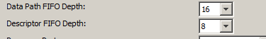 Everything continues to work! Good. Make sure that we provoke the number of accesses to the bus more than the FIFO dimension. Add a hit counter:
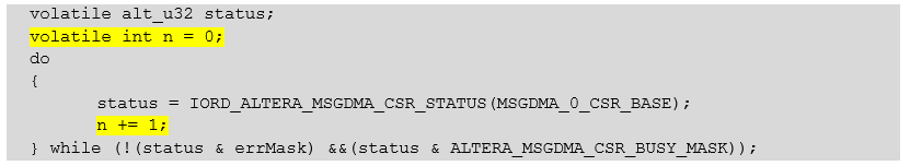
Same text: volatile alt_u32 status;
volatile int n = 0;
do
{
status = IORD_ALTERA_MSGDMA_CSR_STATUS(MSGDMA_0_CSR_BASE);
n += 1;
} while (!(status & errMask) &&(status & ALTERA_MSGDMA_CSR_BUSY_MASK));
At the end of the work, it is 29. This is more than 16. That is, the FIFO should overflow. Just in case, let's add more status register readings. Does not help.With grief, I disconnected from the remote Redd complex, redid the project to my existing breadboard, which I can connect to with an oscilloscope right now (in the office, nobody is at a distance, I can’t reach the oscilloscope). Added two ports to the timer: output clk_copy,
output ready_copy
And appointed them: assign clk_copy = clk;
assign ready_copy = source_ready;
As a result, the module began to look like this:module Timer_ST (
input clk,
input reset,
input logic source_ready,
output logic source_valid,
output logic[31:0] source_data,
   output    clk_copy,
   output    ready_copy
);
logic [31:0] counter;
always @ (posedge clk, posedge reset)
if (reset == 1)
begin
counter <= 0;
end else
begin
counter <= counter + 1;
end
assign source_valid = 1;
assign source_data [31:24] = counter [7:0];
assign source_data [23:16] = counter [15:8];
assign source_data [15:8] = counter [23:16];
assign source_data [7:0] = counter [31:24];
    assign clk_copy = clk;
    assign ready_copy = source_ready;
endmodule
At home I have a smaller model with a crystal, so I had to reduce the appetite of memory. And it turned out that my primitive program would not fit into a 4 kilobyte section. So the topic raised in the last article is, oh, how relevant. Memory in the system - barely enough!When the program starts, we get a ready surge of either 16 or 17 measures. This is filled with the FIFO of the DMA block. The same effect that scared me at the beginning. It is these data that will form the very false buffer filling.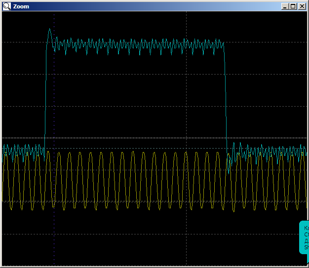 Next, we have a beautiful picture at 40960 nanoseconds, that is, 2048 cycles (with a home crystal, the buffer had to be reduced to 8 kilobytes, that is, 2048 thirty-two-bit words). Here is its beginning:
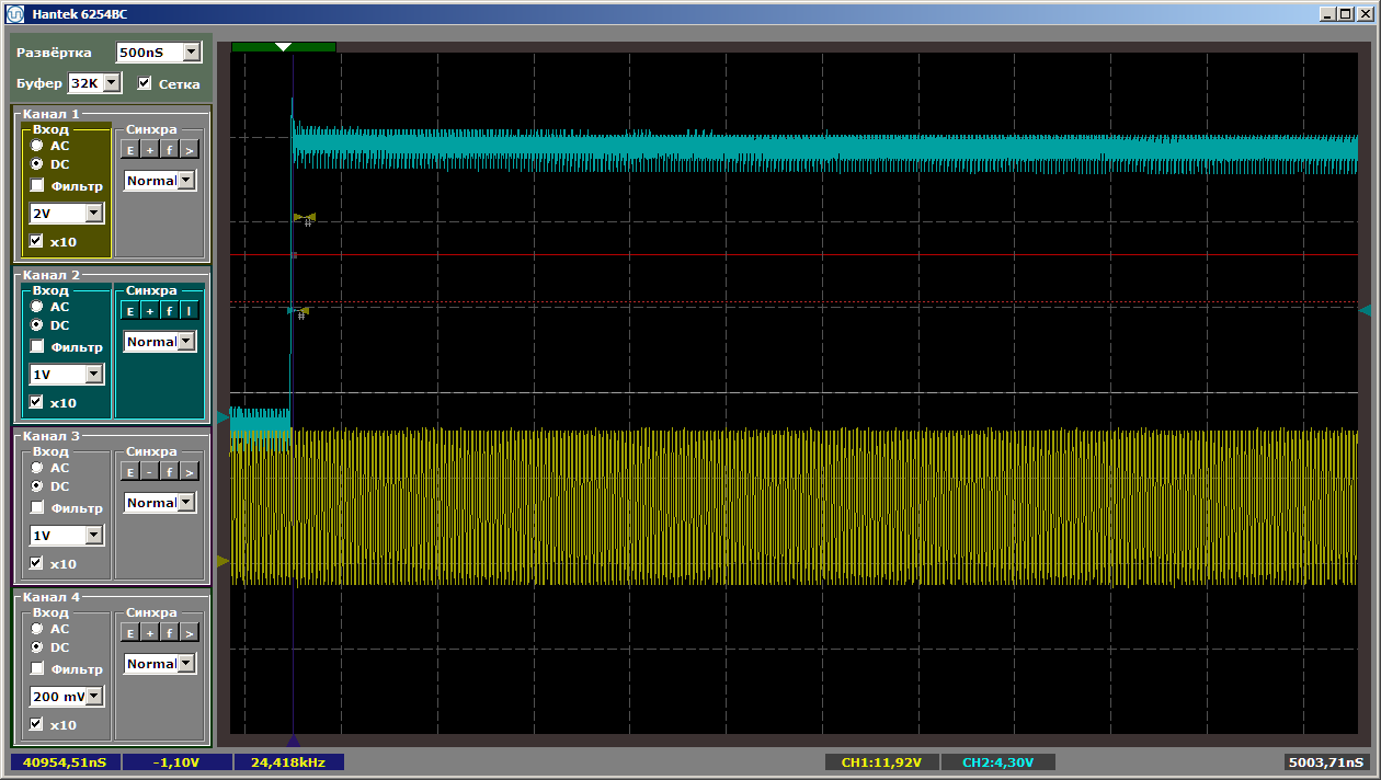 Here is the end:
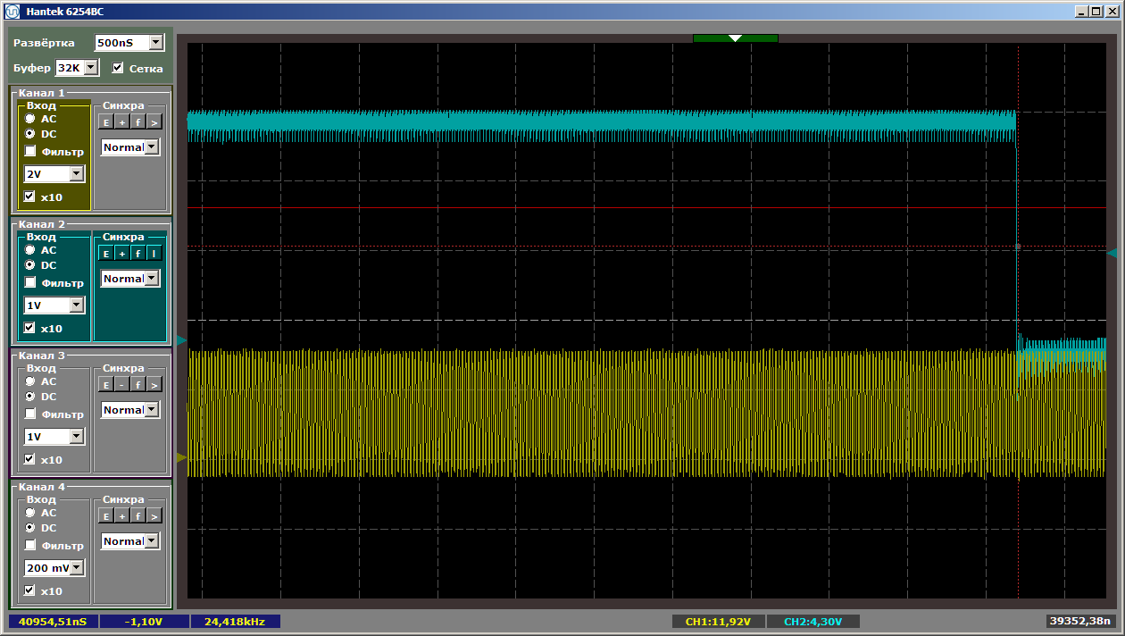 Well, and throughout - not a single failure. No, it was clear that this would happen, but there was some hope ...Maybe we should try to write on the bus, and not just read from it? I added a GPIO block to the system:
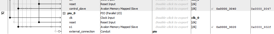 Added an entry to it while waiting for readiness:
Same text volatile alt_u32 status;
volatile int n = 0;
do
{
status = IORD_ALTERA_MSGDMA_CSR_STATUS(MSGDMA_0_CSR_BASE);
IOWR_ALTERA_AVALON_PIO_DATA (PIO_0_BASE,0x01);
IOWR_ALTERA_AVALON_PIO_DATA (PIO_0_BASE,0x00);
n += 1;
} while (!(status & errMask) &&(status & ALTERA_MSGDMA_CSR_BUSY_MASK));
There are no problems and that's it! Who is to blame?There are no miracles, but there are unexplored things
Who is to blame? With grief, I began to study all the menus of the Platform Designer tool and, it seems, found a clue. What does a tire usually look like? The set of wires to which clients are connected. So? It seems so. We see this from the figures in the editor. Just, the second goal of the article was to show how the bus can be divided into two independent segments, each of which works without interfering with the other.But let's look at the messages that appear when the system is generated. Highlight keywords: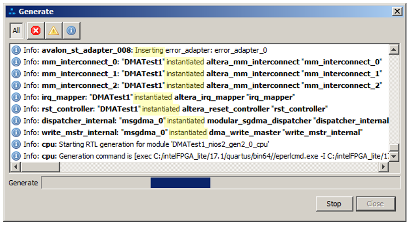 And there are a lot of similar messages: it is added, it is added. It turns out that after editing with pens, a lot of additional things are added to the system. How would you look at a scheme in which all this is already available? I’m still swimming in this, but we can get the most likely answer within the framework of the article by choosing this menu item: The
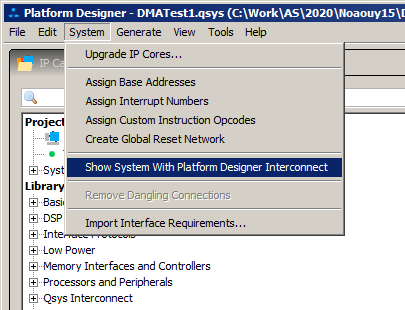 opened picture is impressive by itself, but I won’t give it. And immediately
 I’ll select this tab: And there we see the following: I will
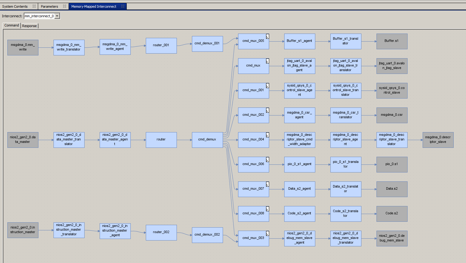 show larger the most important:
 Tires are not combined! They are segmented! I can’t justify it (perhaps experts will correct me in the comments), but it seems that the system inserted the switches for us! It is these switches that create the isolated bus segments, and the main system can work in parallel with the DMA unit, which at this time can access memory without conflict!
We provoke real problems
Having received all this knowledge, we conclude that we can very well provoke problems. This is necessary in order to make sure that the test system can create them, which means that the development environment really resolves them independently. We will not refer to abstract devices on the bus, but to the same Buffer memory so that the cmd_mux_005 block distributes the bus between the processor core and the DMA block. We rewrite the long-suffering wait function like this: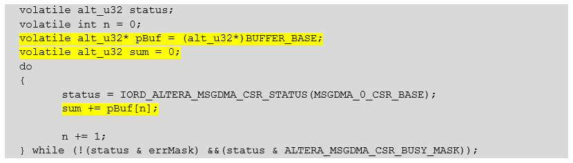
Same text volatile alt_u32 status;
volatile int n = 0;
volatile alt_u32* pBuf = (alt_u32*)BUFFER_BASE;
volatile alt_u32 sum = 0;
do
{
status = IORD_ALTERA_MSGDMA_CSR_STATUS(MSGDMA_0_CSR_BASE);
sum += pBuf[n];
n += 1;
} while (!(status & errMask) &&(status & ALTERA_MSGDMA_CSR_BUSY_MASK));
And finally, dips appeared on the waveform! The memory check function also found a lot of omissions:
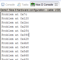 Yes, and we see very well that the data is shifted from row to row:
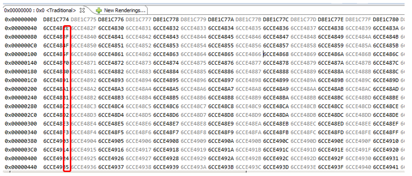 And here is an example of a specific bad spot (6CCE488F is missing):
 Now we see that the experiment was done correctly, just the development environment carried out optimization for us. This is the case when I pronounce the phrase “All smartly hurt all steel” not with mockery, but with gratitude. Thanks to the Quartus developers for this matter!
Conclusion
We learned how to insert a DMA block into the system to transfer streaming data to memory. We also made sure that the process of downloading other devices on the bus will not interfere with the download process. The development environment will automatically create an isolated segment that will run in parallel with other sections of the bus. Of course, if someone turns to the same segment, conflicts and time spent on resolving them are inevitable, but the programmer may well foresee such things.In the next article, we will replace RAM with an SDRAM controller, and the timer with a real "head" and make the first logical analyzer. Will it work? I don’t know yet. I hope the problems do not appear.