Self-isolation is the scourge of modern humanity. Here, for example, in the neighboring city, on Fridays and Saturdays, after traditional clapping at 8 pm, they organize balcony concerts. They feel good, their houses are tall and their neighbors are young. Our neighbors are elderly, they don’t want concerts. And the houses are low, which also does not contribute to idleness. Therefore, we are saved as we can.In the afternoon, on a remote site, not so bad. As in the evening, until the children fall asleep. As in the first few days, until the books run out and the series get bored. But a month passes, followed by another. The soul requires old iron. But not just, but with perversion. And I rummaged through the trash bins and found the Zilog Z80 processor there: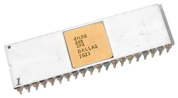 I must say, I really love this processor. Probably the only thing I like about him is the 486th chip, but my hands will not reach it soon, because it’s difficult and pointless to insert it into the breadboard. Have to solder. But I do not want to solder yet. And even more than the Z80 itself, I love the ZX Spectrum computer built on its basis. But the native Spectrum suffers from a misfortune in the form of a ULA custom logic chip, and its clones on the loose side are not particularly difficult to build and refine, but still not for the layout, and indeed, why so many worries when there is arduino?A smart, balanced and adequate reader here will either stop reading or throw something like “1 FPGA microcircuit will accommodate the Spectrum computer class” before stopping. I'm not smart, not adequate, although balanced, but I only know about FPGA that it's cool. I can only do arduino. But really wants to poke the wires in the Z80. Highly.Let's startOf course, let's begin. But first, Disclaimer., , , . — . , , . , (, ?), , , , , . , , , , , .To begin with, what is an adequate 8-bit computer. This is, in fact, a processor connected to ROM and RAM, and on the side is a couple of counters to display on the composite screen. Sometimes, a timer to squeak. ZX Spectrum is no different from the traditional scheme, except for one but. There is a ULA. This, in fact, is the “chipset” of the Spectrum. ULA manages peripherals, such as a tape recorder, tweeter, keyboard (partially), output to the screen (yes, yes, the integrated video card appeared in the Spectrum chipset before it became mainstream). There was also a shared memorial, the first 16 KiB of RAM (addresses from 0x4000 to 0x5B00). From it, the ULA drew a composite onto the screen, and so that the Z80 would not fumble there when it was not necessary, the ULA could stop the processor, if necessary, because the clock signal on the Z80 came from it. That is, if ULA worked with memory, and detected,that the processor also creeps into this memory (for this, it constantly monitored the MREQ and the A15 and A14 lines), it simply stopped the processor clocking until it itself finished doing what it needed. By the way, in order to avoid data corruption on the bus, parts of the bus on the processor side and on the ULA side were delimited by ... resistors ... Moreover, the memory was sitting on the bus from the ULA side and, accordingly, in the event of a collision, completely ignored the data and address from the processor side.completely ignored the data and address from the processor.completely ignored the data and address from the processor.In addition, the Spectrum had ROMs (addresses 0x0000 - 0x3FFF) and its own processor memory (0x8000 - 0xFFFF), to which ULA did not have access, and which worked faster than 16 KiB of shared memory, since the processor did not interfere with ULA in this area . But that was only on the 48K version of the computer. In the basic version, there were only ROMs and 16 KiB compatible with ULA. We’ll start with her.It’s convenient that the Z80 processor can regenerate DRAM, but somehow I don’t want to bother with it, because SRAM is easier to find and I don’t have a multiplexer (or I can’t find it). So, we will use SRAM. To begin with, we will assemble the main skeleton, on which then everything else can be hung. The skeleton will be a processor, ROM with firmware, mapped to the address of the Spectrum's ROM, RAM, mapped to the first 16 KiB after the ROM and some chips to wrap everything ... I must say that for a long time I did not want to rotate, because I have Chinese layouts $ 1 for 2 pieces in ibee. But, for me, the fuss is worth it. If you do not want to mess around for a long time, take good layouts.So, install the Z80.As you can see from the datasheet ,
 The processor has 40 pins divided into groups: address bus, data bus, system control, processor control, processor bus control, well, power and clock. Not all of these conclusions are used in real systems, such as the ZX Spectrum, as can be seen from the diagram.. Of the group "processor control" in the Spectrum, only INT and RESET signals are used. Signal M1 is not used from the “system control” group, the “bus control” group is not used at all. There is a reason for this. The old 8-bit systems were very simple, and the Spectrum was created with the idea of being as simple as possible and everything that could be ignored was ignored. Of course, peripheral manufacturers could use interrupts (INT and NMI signals), they were routed to the expansion slot, but NMI was not used in the spectrum itself. As can be seen from the above diagram, the NMI, WAIT, BUSREQ signals are pulled up by power resistors, since these are low-level activated inputs (this is indicated by the bar above the signal name), and there must be a logical unit (i.e. + 5V) so that God forbid the unnecessary signal did not work. And here are the findings, BUSACK, HALT, M1,and hang in the air, not connected to anything. By the way, note that there is no reset button in the Spectrum. The reset pin is connected viaRC chain to power (RESET is also activated by a low level), since, according to the datasheet, after turning on RESET, at least 3 clock cycles must be active for the processor to enter the operating mode. This RC-circuit keeps a low level until the capacitor is charged to a high level through a resistor.Let's briefly go over the rest of the signals:M1. We do not need. He reports that the processor began to execute the next instruction.MREQ. I need it. It reports that the processor is accessing memory. If this signal becomes low (that is, connected to the power ground), then we will need to activate the memory connected to the processor.IOREQ . I need it. It reports that the processor is accessing a peripheral device. For example, to the keyboard.RD . I need it. Informs that the processor will read data from memory (if MREQ is active) or peripherals (IOREQ).Wr . I need it. Reports that the processor will write data to memory / peripherals.RFSH . I need it. In general, this signal is needed for dynamic memory (DRAM). I do not plan to use it, since its addressing is more difficult (matrix, not linear, that is, it will be necessary to install a multiplexer), and in general, in our time, low-capacity SRAM microcircuits are easier to get. But since the processor itself regenerates DRAM by sorting addresses on the memory bus, this signal will allow us to ignore the regeneration cycles and not activate the memory with active RFSH.HALT . Not needed. Indicates that the processor is stopped.WAIT. Not needed. This signal is needed to ask the processor to stop and wait a bit. Usually used by slow peripherals or memory. But not in the Spectrum. When in the Spectrum peripherals (ULA) decides to stop the processor, then it simply ceases to send a clock signal to it. This is more reliable, because after receiving WAIT, the processor does not immediately stop.INT . Interrupt. It is not clear yet. We assume that it is not needed yet. Then we'll figure it out.The NMI . Unmaskable interruption. Super interrupt. Not necessary.RESET . Without it, it won’t fly.BUSREQ . Not needed. Asks the processor to disconnect from the data / address buses, as well as the control signals. It is necessary if some device wants to gain control over the bus.BUSACK. Not needed. Serves to inform the device that performed BUSREQ that the bus is free.The CLOCK . Clock signal. Clearly, he is needed.Meals are also needed. Glory to the developers, only + 5V / GND. No 3 stresses for you.A0-A15 is the address bus. On it, the processor displays either a memory address (MREQ is active) or an I / O port address (IOREQ is active) with appropriate calls. As you can see, the bus is 16 bits wide, which allows you to directly address 64 KiB of memory.D0-D7 - data bus. The processor outputs to it (WR active), or reads from it (RD active) the requested data.So, we will place the processor on the breadboard. So his conclusions are physically located:
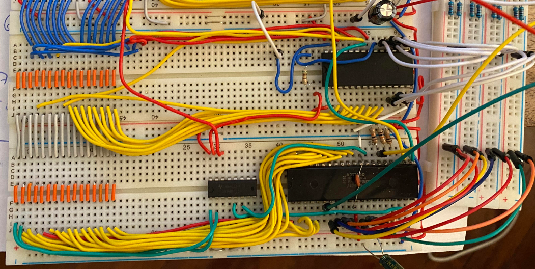
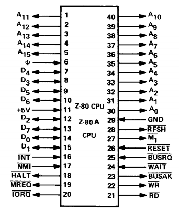 Connect the power (pin 11 and 29). Just in case, I also put a 10 pF capacitor between these legs. But he did not help me in the end. Pins 27, 23, 18 may remain unconnected to anything. Pins 26, 25, 24, 17, 16 are connected via resistors (I used 10 kOhm) to the power supply. I brought the address bus (pins 1-5 and 30-40) to the opposite side of the breadboard, and the data bus (pins 7-10 and 12-15) to a separate data bus made from prototype power buses.Pins 6 (clock signal) and 26 (RESET) are connected (later) to Arduin so that you can control the processor from it.It turned out like this:
 Until you pay attention to the wires from above, they go from the ROM, we will move on to it a bit later. Also, in the photo next to the processor, one more chip is visible. We need it to decode the upper bits of the address. As I said above, there are 3 types of memory in the Spectrum. The lower 16 KiB of the address space is ROM. Accordingly, if the terminals A14 and A15 are in a low state (0 Volts), we need to disconnect everything except the ROM chip from the bus. Next up is 16 KiB of shared memory. Accordingly, we need to connect this memory to the bus (and disconnect the rest) if the output A15 is low and A14 is high (+5 Volts). Well, then comes 32 KiB of fast memory. We will attach this memory later, and we will activate it if the output A15 is in a high state. In addition, do not forget that we only activate memory when active (here, active - low,0 Volt) MREQ and inactive (here, inactive - high, + 5V) RFSH. All this is quite simple to implement on standard logic, on the same NANDs, such as 74HC00, or Orthodox K155LA3, and I understand this task is for the preparatory group of the kindergarten, however, I can only think in truth tables in freedom and in captivityI have a complete Harlequin diagram there , from which you can simply take the part where U4 is drawn (74HC138, fortunately I have about a hundred of them). We will ignore U11 for clarity, since the upper 32KiB are not of interest to us so far.Connecting is very simple.
 As can be seen from the brief descriptionThe microcircuit is a decoder that receives binary numbers from 000 to 111 on the terminals 1 through 3 and activates one of 8 outputs (legs 7 and 9 to 15) corresponding to this number. Since only 8 different numbers can be stored in 3 bits, there are only eight outputs. As you can see, the conclusions are inverted, that is, the one that will be active will have a level of 0V, and all the others + 5V. In addition, a key in the form of a 3-input gate of type “I” is built into the chip, and two of its three inputs are also inverted.In our case, we connect the decoder itself as follows: the most significant bit (3rd leg) to the ground, there will always be 0. The middle bit is to line A15. There will be 1 only if the processor accesses the upper 32KiB of memory (addresses 0x8000 - 0xFFFF, or 1000000000000000 - 1111111111111111 in binary, when the most significant bit is always set to 1). We connect the least significant bit to the A14 line, where the high level will be in case of accessing either the memory after the first 16 KiB, but up to the top 32 KiB (addresses 0x4000 - 0x7FFF, or 0100000000000000 - 0111111111111111 in binary form), or to the most recent 16 KiB of the address spaces (addresses 0xB000 - 0xFFFF, or 1100000000000000 - 1111111111111111 in binary form).Let's see what the output will be in each of the cases:
- 14 15 , 16 , , 000, 0 ( ), Y0 (15 ). , .
- 14 , 15 — , 16 , 32 , 001, 1 , Y1 (14 ). , 16 , .
- 14 , 15 — , - 32 48 , 010, Y2 (13 ). , .
- If both lines (A14 and A15) are active, the processor accesses the top 16 KiB of memory, from 48 to 64 KiB, we don’t have it, so the Y3 pin (12th pin) is also in the air.
In addition, thanks to another element, the microcircuit will activate its findings only if inputs 4 and 5 are low and 6 are high. The 4th input is always in the low state (it is connected directly to the ground), the 5th will only be low when the processor is accessing memory (remember, MREQ in the low state means accessing the memory), and the 6th will be high when the processor does not perform an update cycle DRAM (we have SRAM, so DRAM update cycles are the safest way to just ignore). It turns out great.Next, put the ROM.I took the W27C512 because it’s cheap, cheerful, everything will fit and you can also bank. 64KiB! 4 firmware can be uploaded. Well, I have about a million of these microcircuits. I decided that I would only sew the upper half, since on Harlequin the A15 leg is tied to + 5V, and the A14 is adjustable with a jumper. Thus, I can test the firmware on Harlequin so as not to mess around for a long time. Smorim datasheet . We put the chip on the breadboard. Again, I put it in the right corner to place the address bus on the left. We pull leg A15 to power, A14 wiring to the ground. Wiring - this is so that you can change the memory banks. Since the A15 will always be at a high level, only the top 32 KiB flash drives will be available to us. Of these, the A14 line will select the upper (+ 5V) or lower (ground) 16 KiB. In them, I filled the test image with the programmerand 48K BASIC firmware .The remaining 14 address lines (A0 - A13) are connected to the address bus on the left. We connect the data bus (Q0 - Q7) to our improvised bus in the form of power buses from the breadboard models. Do not forget about food!Now the control signals. OE is an output enable. We need the ROM to send data to the data bus when the processor reads it. So we connect directly to the output of the RD processor. Conveniently, both pins, both OE on ROM and RD on the processor, are active in a low state. This is important; you don’t need to invert anything. In addition, the ROM has a CS input, also active in a low state. If this input is not active, the ROM will ignore all other signals and will not output anything to the data bus. We will connect this input to the Y0 pin (15 pin) of the 74HC138 chip, which is also active in the low state. In the Harlequin circuit, this signal, for some reason, is connected through a resistor. We will do the same. Why, I don’t know. Maybe smart people tell me in the comments ... They told me. Thank,sterr:. , «» . .
 All.Now RAM.It is more difficult with it, since not only the processor, but also ULA, or, in our case, Arduino, work with RAM (with our 16 KiB). Since it is necessary to read something that is displayed on the screen. Therefore, we need to be able to disconnect control signals and the RAM address bus from the processor. We will not disconnect the data bus, we will act as in the original spectrum (and in Harlequin): we will divide the bus with resistors (470-500 Ohms). On the one hand, the resistors will be the processor and ROM, on the other hand, RAM and Arduino. Thus, in the event of a conflict on the data bus, it will work as 2 separate buses. But for the rest we use 74HC245 , as in Harlequin (U43, U44 in the diagram), although in the present Speccythere were also resistors (between IC1 on the one hand, this is ULA, and IC3, IC4 on the other).The 74HC245 is an 8-bit bus buffer. But we have 2 control signals (RD - in the case of reading from memory and CE for activating the RAM itself. We will deal with WR in the case of writing to memory later) and 14 bits of the address: remember, above we already generate a signal to the memory using 74HC138 only in the event that the processor activated A14 with A15 inactive, so we do not need to do any additional decoding of the address, the memory will work only when accessing the first 16 KiB after the ROM. Well, of course, to address 16 KiB you need just 14 address lines (A0-A13). In total, 16 signals are obtained, so we need 2 74HC245 microcircuits. We connect them to the breadboard on the left, in place of the address bus.From the datasheet on the 74HC245 it is clear that, in general, it doesn’t matter which side to connect the microcircuits to, but since I started to build up the layouts from the bottom up, and all the other microcircuits are installed with the first pin to the left, the address bus will connect to side A (pins 2 -9 chips, in the datasheet are designated as A0-A7). The transfer direction is always from the processor to the RAM, since the RAM never sets the address, but only receives it. In the 74HC245, pin 1 (DIR) is responsible for the direction of transmission. According to datasheetso that on the B side there is an output equal to the input on the A side, the DIR must be set to HIGH. So connect the 1st pin of both circuits to + 5V. OE (20th pin, activated by a low level) is connected using wiring to the ground so that it can be quickly switched to + 5V and disconnected from the processor. Further simpler. Connect the power for both chips. The rightmost pins of the right microcircuit (8th and 9th pins, inputs A6 and A7) will be control signals. I connected A7 to the RD terminal of the processor, and A6 to the Y1 pin of the 74HC138 chip, since there will be a low level only when the processor accesses our RAM. The remaining conclusions from side A of both microcircuits (legs 2–9 for the left and legs 2–7 for the right) I connected to the address bus, terminals A13-A0. We do not need the upper 2 bits of the address, because they are already decoded in the signal from the 74HC138.Now about the RAM itself. Naturally, I used what I already had: a cache chip from the old motherboard. I came acrossIS61C256 at 20 ns, but any will do. Speccy worked at a frequency of 3.5 MHz, but for now we will generally be treating Arduinki. If 100 kHz comes out, there will be happiness! So, we connect. Of course, do not forget about food. Conclusions I / O0 - I / O7 are connected to the breadboard of the data bus AFTER the resistors. I was lucky (in fact, not), on my Chinese mockups, the power buses are divided exactly in the middle. I used this feature to separate the bus with resistors. If your layouts are wrong, you have to be
 pervertedmake a second data bus, and connect it with resistors to the first. The conclusions of A0-A13 are thrown at the corresponding B-conclusions of the 74HC245 chips, not forgetting that the rightmost ones are connected not to the data bus, but to the control signals. A14 - by choice, either to the ground, or to + 5V. A 32 KiB chip, so this conclusion will determine which half we will use. If you find a 16 KiB SRAM, there will be no A14 line in it. The outputs are WE (write enable), CE (chip enable) and OE (output enable). All are activated low. OE must be connected to the processor’s RD, but, of course, not directly, but through the right 74HC245, where the RD comes to my A7 foot, and accordingly comes out of the B7 foot (11th pin). There and connect. CE must be connected to Y1 from the 74HC138, which decodes the address. Her signal comes to me on the A6 of the right chip 74HC245, respectively,comes out of foot B6 (12 pins). WE I directly connected to the output of the WR processor. I also installed a jumper wire from the OE signal and stuck it just in the unused part of the layout. By connecting this wire to the power ground, I can force the RAM to be activated when I read it from Arduinka. Still, I pulled all the control signals of the RAM to + 5V using resistors of 10 kOhm. Just in case. It turned out like this: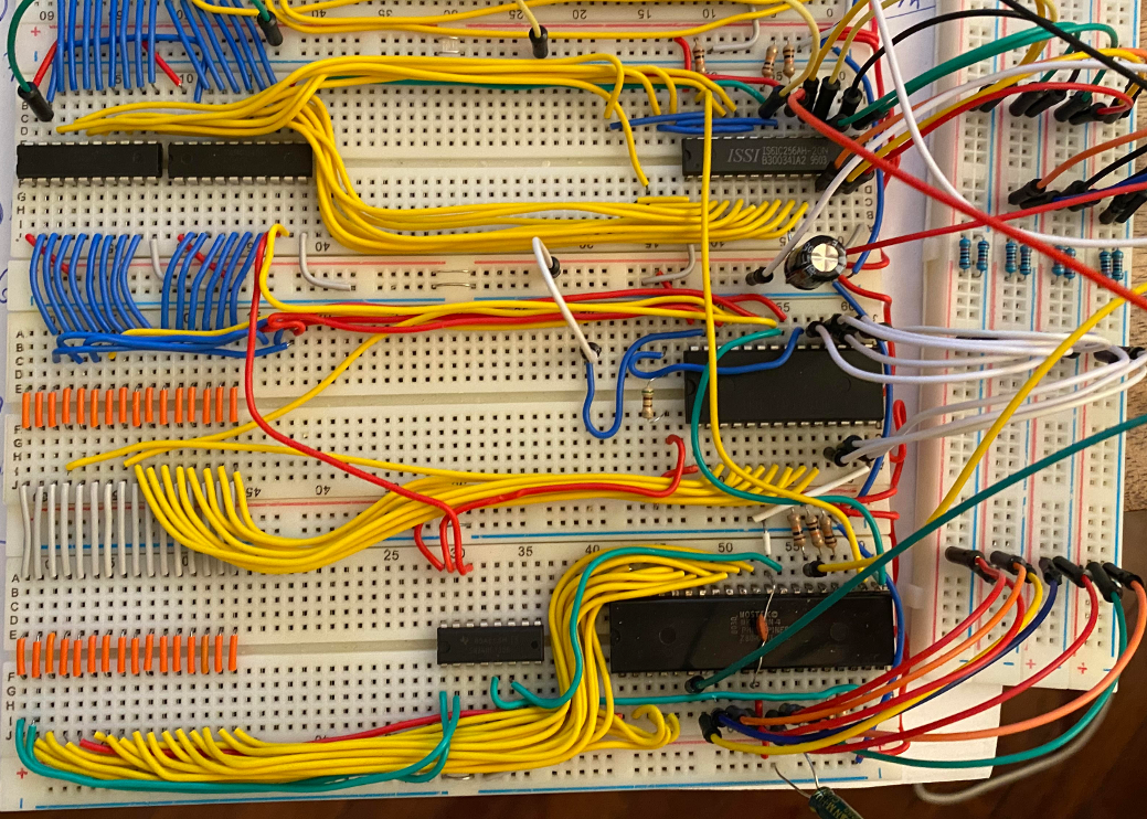 In general, here, and if at all, at the very beginning, there should be an educational program on the timing of signals on the tires. I will not do this, since it has been done many times on the network by much more intelligent people than me. For those interested, I can recommend this video:In general, if you are not subscribed to this channel and are interested in electronics as an amateur, and not as a professional, I highly recommend it to you. This is a very high quality content.In general, that’s almost all. Now you just need to understand how to read data from RAM in Arduino. To begin with, let's calculate how many Arduinki conclusions we need. We need to give a clock signal and control the RESET, these are 2 pins. 8 bits of data bus - another 8 pins. Plus 13 bits of address, total 23 pins. In addition, we need to communicate with Arduinka, we will do this through her serial interface, this is another 2 pins. Unfortunately, there are only 20 conclusions on my DNA.Well, it doesn’t matter. I do not know a single person who has Arduino and does not have 74HC595. It seems to me that they are sold only in the kit. At least I only have 74HC00 chips more than 595x. So we use them. Moreover, I will save space in the article, because the work of the 595x with arduino is perfectly described here. 595mi we will generate the address. The chip will need 2 pieces (since we have 13 bits of the address, and the 595th has 8 pins). How to connect several 595x for bus expansion is described in detail at the link above. I only note that in the examples at that link OE (pin 13) 595x is pulled to the ground. We categorically will not do this, we will send a signal from Arduinki there, since the 595x pins will be connected directly to the RAM address bus, and we do not need any spurious signal there. After connecting the 595x pins to the RAM address bus, nothing more needs to be done on the mock-ups. Time to connect the arduinka. But first, write a sketch:
#define CPU_CLOCK_PIN 2
#define CPU_RESET_PIN 3
#define RAM_OUTPUT_ENABLE_PIN 4
#define RAM_WRITE_ENABLE_PIN 5
#define RAM_CHIP_ENABLE_PIN 6
#define RAM_BUFFER_PIN 7
#define SR_DATA_PIN 8
#define SR_OUTPUT_ENABLE_PIN 9
#define SR_LATCH_PIN 10
#define SR_CLOCK_PIN 11
void setup() {
DDRC = B00000000;
pinMode(CPU_CLOCK_PIN, INPUT);
pinMode(CPU_RESET_PIN, INPUT);
pinMode(RAM_WRITE_ENABLE_PIN, INPUT);
pinMode(RAM_OUTPUT_ENABLE_PIN, INPUT);
pinMode(RAM_CHIP_ENABLE_PIN, INPUT);
pinMode(RAM_BUFFER_PIN, OUTPUT);
digitalWrite(RAM_BUFFER_PIN, LOW);
pinMode(SR_LATCH_PIN, OUTPUT);
pinMode(SR_CLOCK_PIN, OUTPUT);
pinMode(SR_DATA_PIN, OUTPUT);
pinMode(SR_OUTPUT_ENABLE_PIN, OUTPUT);
digitalWrite(SR_OUTPUT_ENABLE_PIN, HIGH);
Serial.begin(9600);
Serial.println("Hello");
}
void shiftReadValueFromAddress(uint16_t address, uint8_t *value) {
pinMode(RAM_WRITE_ENABLE_PIN, OUTPUT);
digitalWrite(RAM_WRITE_ENABLE_PIN, HIGH);
pinMode(RAM_OUTPUT_ENABLE_PIN, OUTPUT);
digitalWrite(RAM_OUTPUT_ENABLE_PIN, HIGH);
digitalWrite(SR_LATCH_PIN, LOW);
shiftOut(SR_DATA_PIN, SR_CLOCK_PIN, MSBFIRST, address>>8);
shiftOut(SR_DATA_PIN, SR_CLOCK_PIN, MSBFIRST, address);
digitalWrite(SR_LATCH_PIN, HIGH);
digitalWrite(SR_OUTPUT_ENABLE_PIN, LOW);
digitalWrite(RAM_OUTPUT_ENABLE_PIN, LOW);
delay(1);
DDRC = B00000000;
*value = PINC;
digitalWrite(RAM_OUTPUT_ENABLE_PIN, HIGH);
digitalWrite(SR_OUTPUT_ENABLE_PIN, HIGH);
pinMode(RAM_WRITE_ENABLE_PIN, INPUT);
pinMode(RAM_OUTPUT_ENABLE_PIN, INPUT);
}
void runClock(uint32_t cycles) {
uint32_t currCycle = 0;
pinMode(CPU_CLOCK_PIN, OUTPUT);
while(currCycle < cycles) {
digitalWrite(CPU_CLOCK_PIN, HIGH);
digitalWrite(CPU_CLOCK_PIN, LOW);
currCycle++;
}
pinMode(CPU_CLOCK_PIN, INPUT);
}
void trySpectrum() {
pinMode(RAM_WRITE_ENABLE_PIN, INPUT);
pinMode(RAM_OUTPUT_ENABLE_PIN, INPUT);
pinMode(CPU_RESET_PIN, OUTPUT);
digitalWrite(CPU_RESET_PIN, LOW);
runClock(30);
digitalWrite(CPU_RESET_PIN, HIGH);
runClock(12500000);
}
void readDisplayLines() {
uint8_t value;
digitalWrite(RAM_BUFFER_PIN, HIGH);
pinMode(RAM_CHIP_ENABLE_PIN, OUTPUT);
digitalWrite(RAM_CHIP_ENABLE_PIN, LOW);
for(uint16_t i=16384; i<16384+6144;i++) {
shiftReadValueFromAddress(i, &value);
Serial.println(value);
}
pinMode(RAM_CHIP_ENABLE_PIN, INPUT);
}
void loop() {
trySpectrum();
Serial.println("Hope we are ok now. Please set up memory for reading");
delay(40000);
Serial.println("Reading memory");
readDisplayLines();
Serial.println("Done");
delay(100000);
}
As you can see from the sketch (well, really, suddenly, someone read it), I read the data bus to port C. As Arduischik can remember, in CID port C is 6 pins. That is, I read only 6 bits. Yes, for the simplicity of the process, I ignore the 2 high bits in each byte of the screen buffer. This will result in the fact that every 2 pixels after 6 there will always be background colors. While a ride, then fix it. This is the skeleton.Now for the connection itself. In principle, everything is painted at the very top of the sketch:// CPU defines
#define CPU_CLOCK_PIN 2 - 2 6 ( )
#define CPU_RESET_PIN 3 - 3 26 (RESET)
// RAM defines
#define RAM_OUTPUT_ENABLE_PIN 4 - 4 22 (OE)
#define RAM_WRITE_ENABLE_PIN 5 - 5 . .
#define RAM_CHIP_ENABLE_PIN 6 - 6 . , . - , - . , .
#define RAM_BUFFER_PIN 7 - , 6, .
// Shift Register defines
#define SR_DATA_PIN 8 - 8 14 "" 595. 9 , .
#define SR_OUTPUT_ENABLE_PIN 9 - 13 595
#define SR_LATCH_PIN 10 - 12 595
#define SR_CLOCK_PIN 11 - 11 595.
Everything is simple. Here's how it looks like everything in my collection (the arduinka was cut in the picture, but there isn’t much to see):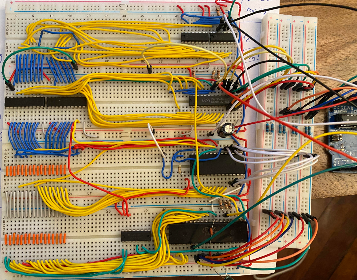 At startup, Arduino cheerfully says Hello to the serial port of the computer (albeit virtual), and starts tormenting the processor. Having thoroughly tortured him (a couple of minutes), the program will stop the poor guy and will offer you to rearrange the jumpers with the pens on the breadboard, disconnecting the memory from the address bus and processor control signals.Now we need to use the handles to rearrange the wiring connected to pins 19 of both 74HC245 from the ground to + 5V. Thus, we disconnect the processor from RAM. Pin 22 of the RAM chip itself must be connected to the ground (I wrote above about the wiring, which I just stuck in the breadboard so far, in an unused place). Thus, we forcibly turn on the RAM.After that, having waited a little, Arduinka will begin to read the contents of the memory and output it in a column to the serial port. There will be many, many numbers. Now you can copy this data from there and paste it, say, into a text file, without forgetting to clean up all unnecessary text (a couple of lines at the top, and “Done” at the bottom), we only need numbers. This is what our Speccy recorded in video memory. It remains only to see what was there in the video memory. And the Spectrum’s video memory is not easy ...As you can see, the pixels themselves are stored separately from the color. We will ignore the color for now, let's read only the pixels themselves. But they are not so easy to decode. After much pain in Visual Studio, I came to this elegant solution:
#include "stdafx.h"
#include <windows.h>
#include <stdint.h>
#include <stdio.h>
LRESULT CALLBACK WndProc(HWND, UINT, WPARAM, LPARAM);
uint8_t *scrData;
VOID OnPaint(HDC hdc) {
size_t arrSize = 6144;
for (size_t arrPos = 0; arrPos < arrSize; arrPos++) {
int blockPos = arrPos % 2048;
int currBase = (blockPos % 256) / 32;
int currX = blockPos % 32;
int currBlock = arrPos / 2048;
int currRow = blockPos / 256;
int currY = currBlock * 64 + currBase * 8 + currRow;
for (int trueX = 0; trueX < 8; trueX++) {
char r = ((scrData[arrPos] >> trueX) & 1)*255;
SetPixel(hdc, currX * 8 + (8-trueX), currY, RGB(r, r, r));
}
}
}
void loadData() {
FILE *file;
errno_t err;
if ((err = fopen_s(&file, "data.txt", "r"))) {
MessageBox(NULL, L"Unable to oopen the file", L"Error", 1);
}
scrData = (uint8_t*)malloc(6144);
int currDataPos = 0;
char buffer[256];
char currChar = 0;
int currLinePos = 0;
while (currChar != EOF) {
currChar = getc(file);
buffer[currLinePos++] = currChar;
if (currChar == '\n') {
buffer[currLinePos] = 0;
scrData[currDataPos++] = (uint8_t)atoi(buffer);
currLinePos = 0;
}
}
fclose(file);
}
INT WINAPI WinMain(HINSTANCE hInstance, HINSTANCE, PSTR, INT iCmdShow) {
HWND hWnd;
MSG msg;
WNDCLASS wndClass;
wndClass.style = CS_HREDRAW | CS_VREDRAW;
wndClass.lpfnWndProc = WndProc;
wndClass.cbClsExtra = 0;
wndClass.cbWndExtra = 0;
wndClass.hInstance = hInstance;
wndClass.hIcon = LoadIcon(NULL, IDI_APPLICATION);
wndClass.hCursor = LoadCursor(NULL, IDC_ARROW);
wndClass.hbrBackground = (HBRUSH)GetStockObject(WHITE_BRUSH);
wndClass.lpszMenuName = NULL;
wndClass.lpszClassName = TEXT("GettingStarted");
RegisterClass(&wndClass);
hWnd = CreateWindow(
TEXT("GettingStarted"),
TEXT("Getting Started"),
WS_OVERLAPPEDWINDOW,
CW_USEDEFAULT,
CW_USEDEFAULT,
CW_USEDEFAULT,
CW_USEDEFAULT,
NULL,
NULL,
hInstance,
NULL);
loadData();
ShowWindow(hWnd, iCmdShow);
UpdateWindow(hWnd);
while (GetMessage(&msg, NULL, 0, 0)) {
TranslateMessage(&msg);
DispatchMessage(&msg);
}
return msg.wParam;
}
LRESULT CALLBACK WndProc(HWND hWnd, UINT message, WPARAM wParam, LPARAM lParam) {
HDC hdc;
PAINTSTRUCT ps;
switch (message) {
case WM_PAINT:
hdc = BeginPaint(hWnd, &ps);
OnPaint(hdc);
EndPaint(hWnd, &ps);
return 0;
case WM_DESTROY:
PostQuitMessage(0);
return 0;
default:
return DefWindowProc(hWnd, message, wParam, lParam);
}
}
The program opens the data.txt file from its directory. In this file, the text output of the arduino (after deleting all the extra lines, as mentioned above.)We feed it the resulting file, and as a result: Yes, while the result is very far from ideal, but it is definitely the output to the screen. Moreover, the one that is needed. From ROM with diagnostic firmware.Well, the computer skeleton is ready. Yes, it’s impossible to use it yet, but you can see how extremely simple the old 8-bit computers were arranged. I still beat a little over the breadboard, but the conclusion only got worse. It seems that the next step is to solder on a normal, unsoldered breadboard, with normal power.But is it necessary?