Hi Habr! Once at work, I got the task of assessing the possibility of implementing data storage on an SD card when connecting it to an FPGA. The use of SPI was assumed as an interaction interface, since it is easier to implement. I would like to share the experience gained.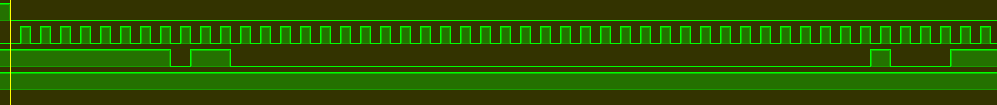 Since the space on the printed circuit board is always limited, consideration of SD-cards will be performed on the example of cards in the microSD form factor.
Content
1. Reading specification1.1 General information1.2 Initialization1.3 Erasing information1.4 Reading information1.4.1 Reading one data block1.4.2 Reading many data blocks1.5 Writing information1.5.1 Writing one data block1.5.2 Writing many data blocks2. Implementing the algorithm in hardware2.1 Component of the physical layer2.2 Component of the command level2.3 Component of communication with the outside world3. Verification in hardware4. Results1. Reading specifications
1.1 General
A quick reading of the specification tells us the following SD card options:- data transfer to the SD card is carried out on one line;
- reading data from an SD card is carried out on one line;
- in SPI mode, the power can be only + 3.3V;
- clock frequency in initialization mode in the range of 100-400 kHz;
- clock frequency after initialization - 25 MHz.
This immediately leads to the point about the theoretical peak bandwidth: 25 MHz * 1 bit = 25 Mb / s, which is somewhat small. The second minus the use of SD-cards, power + 3.3V. On the printed circuit board on which it was planned to install the SD card, there is no such voltage.MicroSD form factor cards can be divided into 3 categories by capacity:- SDSC Card capacity up to 2 GB inclusive. The address inside the card is byte.
- SDHC. The card capacity is more than 2 GB and up to 32 GB inclusive. The address inside the card indicates a 512 byte block.
- SDXC. The card capacity is more than 32 GB and up to 128 TB inclusive. The address inside the card indicates a 512 byte block.
The general view of the map is shown in the figure below.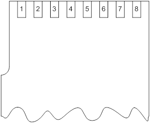 The connection is carried out according to the diagram below:
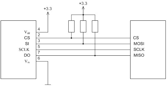 The resistors must be rated at 50 kOhm.After turning on the power, the SD card is in SDIO mode. To switch to SPI mode, you must perform initialization. The protocol for working with the card involves the use of a control scheme for the correct transfer of data and commands in the form of a CRC algorithm. When operating in SPI mode, CRC verification is disabled by default. Thus, the first command sent to the card to switch the card to SPI mode must contain the correct CRC value.Commands transmitted over the SPI interface are 48 bits in size. Command format:
- Bit 47 (leftmost) always contains the value 0.
- Bit 46 always contains the value 1.
- Bits 45..40 contain the command index.
- Bits 39..8 contain the arguments of the command.
- Bits 7..1 contain CRC from previous bits.
- Bit 0 always contains the value 1.
Bits 47 and 46 give the card the ability to unambiguously track the start of a transaction, since the MOSI bus at rest is equal to one. The commands used when working with the SD card will receive answers like R1, R3, R7.
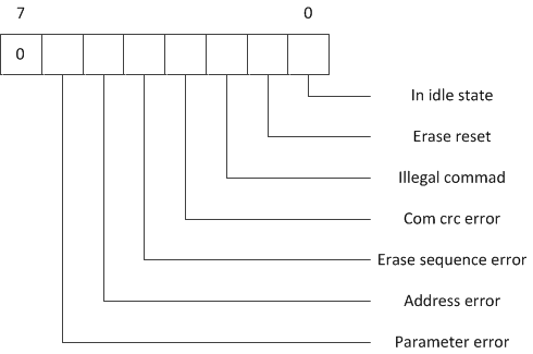 An answer of type R1, size 8 bits. Answer type R3, size 40 bits. Answer type R7, size 40 bits. All commands and their answers are detailed in the Physical Layer Simplified Specification.
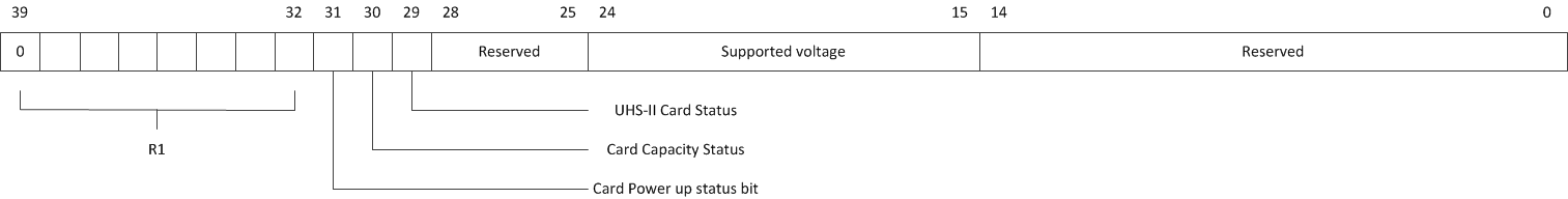

1.2 Initialization
Initialization Algorithm:- After turning on the power, wait at least 1 ms.
- Generate a minimum of 74 clock switching for the card. CS and MOSI lines must be in logical unit state.
- Generate command CMD0. The CMD0 command resets the SD card.
- CMD0. R1. , R1 16 , 3. R1 , 0x01 ( ), 3, 5.
- CMD8. .
- CMD8. R7. , , , 7, , , 17, 13.
- CMD55. CMD55 , .
- CMD55. R1. 0x01 ( ), 7, 9.
- ACMD41. ACMD41 , SDSC ( 0x00000000) .
- ACMD41. R1. , , 11. , 0x00 ( ) 14, 7.
- CMD1. CMD1 ACMD41.
- CMD1. R1. , , 13, , 0x00 ( ), 14, 11.
- . , . .
- CMD16. , 512 .
- CMD16. R1. , 0x00 ( ) 16, 13.
- . . .
- CMD55. CMD55 , .
- CMD55. R1. 0x01 ( ), 17, 19.
- ACMD41. ACMD41. ACMD41 , SDHC ( 0x40000000) .
- ACMD41. R1. , , 13. , 0x00 ( ) 21, 17.
- CMD58. .
- Waiting for a response to CMD58 command. The answer is an R3 type response. If a bit is set in the response that the card works with block addresses of 512 bytes, go to step 16, otherwise to step 14.
After initialization is completed, the card can be operated in blocks of 512 bytes with a clock frequency of 25 MHz. This is the full version of the initialization algorithm, which covers all types of cards. In my case, when using a 16 GB card, the initialization algorithm consisted of steps 1-6, 17-22, 16.1.3 Erasing Information
Micro SD form factor cards support erase commands. After the erase command, the value of the specified erase addresses will be filled with the value 0xFF or 0x00, depending on the card.Information Erasing Algorithm- CMD32. .
- CMD32. R1. 0x00 ( - ), 3, 4.
- . , .
- CMD33. . , CMD32.
- CMD33. R1. 0x00 ( - ), 3, 6
- Sending CMD38 command. The command to erase information from the selected blocks. Any 4 bytes should be sent as an argument, except for the values 0x00000001, 0x00000002.
- Waiting for a response to CMD38 command. The answer is a response of type R1b. This is an extended version of the answer when the card generates an R1 response, and then draws the MISO line to zero, indicating the chip is busy. It is necessary to wait until the unit value appears on the MISO line. If the answer is not 0x00 (there was some error while executing the command), go to step 3, otherwise to step 8
- Completion of the erase algorithm.
1.4 Reading information
Reading information from an SD card via SPI is possible in two ways.1.4.1 Reading a single data block
When reading one data block, the Master device generates a command for the SD card to read one data block, awaits a response that the command has been processed and is waiting for a packet with data from the card. After receiving a packet with data from the card, the read transaction ends.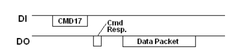 General view of a transaction reading one block of data.Initially, such an option was implemented, but the resulting speed was very upset (speed comparisons will be lower).
1.4.2 Reading multiple data blocks
When reading multiple data blocks, the Master device generates a command for the SD card to read multiple data blocks, awaits a response that the command has been processed, and expects a packet of data from the card. After sending a data packet, the card sends the next data packet. This will continue until a command is received from the Master device to complete the reading.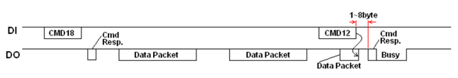 General view of a transaction reading many data blocks.
 Data Packet StructureWhere:
- Data Token The read command uses the value 0xFE.
- Data Block. Contains data read from the card.
- CRC Contain the checksum from the previous fields.
If an error occurred while reading, the card instead of Data Token returns an Error Token. Error Token size is 1 byte. Bits 7..5 contain a value of zero, bits 4..0 encode the type of error.Algorithm for reading multiple data blocks:- Sending CMD18 command. The command tells the card that multiple blocks will be read.
- Waiting for a response to CMD18 command. The answer is an R1 type response. If the answer is not 0x00 (there was some error while executing the command), go to step 3, otherwise to step 4.
- Error status. Reading failed, exiting the reading algorithm.
- Waiting for a token from the card. If an Error Token is received from the card, go to step 3, otherwise go to step 5.
- Receive from a data block card 512 bytes in size.
- Receive from the card CRC field size of 2 bytes.
- . , 8, 4.
- CMD12. . , Data Packet, .
- CMD12. R1b. R1, MISO , . MISO , . 0x00 ( - ), 3, 10.
- .
There is a slight nuance in the reading algorithm. The chip select signal (CS) must be set to logic zero before generating the CMD18 command and set to logic one after receiving a response to the CMD12 command.1.5 Recording Information
Writing information to the SD card via the SPI interface is possible in two versions.1.5.1 Writing a single data block
When recording one data block, the Master device generates a command for the SD card to write one data block, awaits a response from the card that the command has been processed, transmits a packet with data for recording to the card, expects a response from the card that the data is written, completes the transaction. General view of a write transaction of one data block.As with reading, a record of one data block was originally implemented. The speed results were unsatisfactory.
1.5.2 Writing multiple data blocks
When recording multiple data blocks, the Master device generates a command to record multiple data blocks, awaits a response from the card that the command has been processed, transmits a packet with data for recording to the card, expects a response from the card that the data is recorded. After receiving a Master response, the device transmits a packet with the following data for recording to the card. This will continue until the Master device sends a Stop Data Token.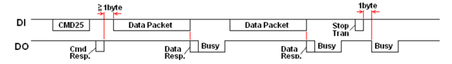 General view of a write transaction for multiple data blocks.The structure of the Data Packet is similar to the structure of the Data Packet when reading data.Format:
- Data Token For the write command, the value 0xFC is used.
- Data Block. Contains data written to the card.
- CRC Contain the checksum from the previous fields.
The Stop Tran Token used to complete the write command is 1 byte in size and equal to 0xFD.After the last bit of the Data Packet has been pushed into the card, the card responds to the next clock with the status of the data record - Data Response. Data Response has a size of 1 byte, bits 7..5 can be any, bit 4 is always zero, bit 0 is always equal to one, bits 3..1 encode the status of the data record. After the card has returned the Data Packet, the card draws the MISO line to zero, indicating the card is busy. After the logical unit level is on the MISO line, you can transfer the next data packet to the card.The algorithm for recording multiple data blocks:- Sending CMD25 command. The command tells the card that multiple blocks will be written.
- CMD25. R1. 0x00 ( - ), 3, 4.
- . , .
- .
- 512 .
- CRC 2 .
- Data Response . , 3, 8.
- . , 9, 4.
- Stop Tran Token. , .
- Waiting for a response from the card. The card on Stop Tran Token draws the MISO line to zero, indicating the card is busy. It is necessary to wait on the MISO line for the unit value, which will indicate the end of the command
- The completion of the recording algorithm.
There is also a small nuance in the recording algorithm. The chip select signal (CS) must be set to logic zero before generating the CMD25 command and set to logic one after receiving a response to Stop Tran Token2. Implementation of the algorithm in hardware
As a result of reading the specification, we get some characteristics of the algorithm that need to be implemented in the hardware.Possible operating modes:- Initial frequency formation. CS and MOSI lines must be in logical unit state.
- Transfer data to an SD card.
- Receive data from an SD card.
- Waiting for the completion of the team. It is used when, after generating a response, the SD card draws the MISO line to zero in order to wait for the appearance of a unit.
- Read response when writing data.
- Waiting for a token while reading data.
Possible clock modes:- Clock signal to initialize.
- Clock signal for work.
From my point of view, the algorithm is optimally implemented using three components:- The component of the physical layer, which is connected directly to the SD card, generates SCLK, CS, DI signals, reads with DO.
- A command-level component that prepares all the data for a component in the physical layer.
- A component of communication with the outside world that hides the entire internal device and provides an interface for commands (reading, writing, erasing) and data.
2.1 Physical layer component
entity SDPhy is
generic ( gTCQ : time := 2 ns );
port (
iPhyTxData : in std_logic_vector( 9 downto 0);
iPhyMode : in std_logic_vector( 4 downto 0);
iPhyTxWrite : in std_logic;
oPhyTxReady : out std_logic;
oPhyRxData : out std_logic_vector( 7 downto 0);
oPhyRxWrite : out std_logic;
oPhyCmdEnd : out std_logic;
oSdCS : out std_logic;
oSdClk : out std_logic;
oSdMosi : out std_logic;
oSdMosiT : out std_logic;
iSdMiso : in std_logic;
sclk : in std_logic;
pclk : in std_logic;
rst : in std_logic );
end SDPhy;
Where:- iPhyTxData , iPhyMode , .
- iPhyTxWrite , iPhyTxData iPhyMode .
- oPhyTxReady , . FULL FIFO, .
- oPhyRxData , SD-.
- oPhyRxWrite , oPhyRxData .
- oPhyCmdEnd , .
- oSdCS (CS) SD-.
- oSdClk SD-.
- oSdMosi SD-.
- oSdMosiT SD-.
- iSdMiso SD-.
- sclk SD- (50 ).
- pclk , .
- rst reset signal, active level one.
In FPGAs, there are special units for working with a clock signal (PLL, MMCM), however, receiving a clock signal less than 5 MHz from their output is problematic. As a result, the physical layer operates at a frequency of 50 MHz. Together with each data in the iPhyMode signal, a bit is received that indicates at what frequency these data should be transferred to the SD card (or received from it). Depending on the speed bit, Clock enable signals are generated.Two automata are implemented in the component of the physical layer, for transferring data to an SD card and for receiving data from it.Machine code for data transfer: github .- SDummy state provides initial frequency shaping, 128 switching.
- STxBits status provides data transfer to the SD card.
The code of the machine for receiving data: github .- The sRxBits state provides data reception from the SD card.
- The sBusy state ensures that the SD card is ready (the card releases the MISO line to unit level).
- The sResp state implements reading the response when writing data.
- The sToken state implements a token wait while reading data.
2.2 Command-level component
entity SdCommand is
generic ( gTCQ : time := 2 ns );
port (
oSdInitComp : out std_logic;
oSdInitFail : out std_logic;
iSdAddress : in std_logic_vector(31 downto 0);
iSdStartErase : in std_logic;
iSdStartRead : in std_logic;
iSdStartWrite : in std_logic;
oSdCmdFinish : out std_logic_vector( 1 downto 0);
oSdhcPresent : out std_logic;
oSdReadData : out std_logic;
iSdDataR : in std_logic_vector(31 downto 0);
oSdWriteData : out std_logic;
oSdDataW : out std_logic_vector(32 downto 0);
oSdCS : out std_logic;
oSdClk : out std_logic;
oSdMosi : out std_logic;
oSdMosiT : out std_logic;
iSdMiso : in std_logic;
pclk : in std_logic;
sclk : in std_logic;
rst : in std_logic );
Where:- oSdInitComp sign completion of initialization of the SD card.
- oSdInitFail sign of initialization failure.
- iSdAddress address in the SD card to execute the command.
- iSdStartErase start erase command execution.
- iSdStartRead start reading command execution.
- iSdStartWrite start write command execution.
- oSdCmdFinish team completion status. The zero bit is equal to one, the command completed successfully. The first bit is one, the command completed with an error.
- oSdhcPresent SDHC / SDXC card detection flag.
- oSdReadData Read data to write to the SD card.
- iSdDataR data for writing to the SD card.
- oSdWriteData flag to write data read from the SD card.
- oSdDataW data read from an SD card.
The remaining signals coincide with the signals of the physical layer.The component has 5 automatic machines.- smSdInit ( github ) - initialization of the SD card.
- smSdErase ( github ) - erase data from an SD card.
- smSdRead ( github ) - read data from an SD card.
- smSdWrite ( github ) - write data to an SD card.
- smSdCommand ( github ) - on the basis of the generated features prepares data for the physical layer from all previous machines.
2.3 Component of communication with the outside world
entity SdHost is
generic ( gTCQ : time := 2 ns );
port (
iSdCommand : in std_logic_vector( 2 downto 0);
iSdAddress : in std_logic_vector(31 downto 0);
iSdStart : in std_logic;
oSdStatus : out std_logic_vector( 1 downto 0);
oSdInitFail : out std_logic;
iSdTxData : in std_logic_vector(31 downto 0);
iSdTxValid : in std_logic;
iSdTxLast : in std_logic;
oSdTxReady : out std_logic;
oSdRxData : out std_logic_vector(31 downto 0);
oSdRxValid : out std_logic;
oSdRxLast : out std_logic;
iSdRxReady : in std_logic;
oSdCS : out std_logic;
oSdClk : out std_logic;
oSdMosi : out std_logic;
oSdMosiT : out std_logic;
iSdMiso : in std_logic;
pclk : in std_logic;
sclk : in std_logic;
rst : in std_logic );
Where:- iSdCommand command code to execute.
- iSdAddress is the address to execute the command.
- iSdStart start command execution.
- oSdStatus team completion status. The zero bit is equal to one - the command is completed. The first bit is one - the command completed with an error.
- oSdInitFail sign of initialization failure.
- iSdTxData. Axi-Stream interface for writing data to an SD card. Port with data.
- iSdTxValid. Axi-Stream interface for writing data to an SD card. Port with a write signal.
- iSdTxLast. Axi-Stream interface for writing data to an SD card. Port with a sign of the last dw in the data.
- oSdTxReady. Axi-Stream interface for writing data to an SD card. Port with a sign of readiness for receiving data.
- oSdRxData. Axi-Stream interface for reading data from an SD card. Port with data.
- oSdRxValid. Axi-Stream interface for reading data from an SD card. Port with a write signal.
- oSdRxLast. Axi-Stream interface for reading data from an SD card. Port with a sign of the last dw in the data.
- iSdRxReady. Axi-Stream interface for reading data from an SD card. Port with a sign of readiness for receiving data.
The remaining signals coincide with the signals of the physical layer.The component implements one smSdControl ( github ) machine .- SIdle state. Waiting for initialization and command to complete.
- The state of sWaitCmd. Checking the type of command.
- sReadCmd. FIFO, , SD- .
- sWriteCmd. , FIFO SD-, .
- sEraseCmd. .
- sWaitEnd. .
- sFinish. , .
3.
The algorithm is written, verified in the simulator. It is necessary to check now in iron. From what was available, the Zybo board from Digilent came up
. It has free FPGA terminals in a bank with a voltage of + 3.3V, to which you can easily connect an external device. Yes, and the type of FPGA used is Zynq-7000, which means there is a processor core. You can write a test in C, which will simplify the testing task. So, we connect the implemented algorithm to the processor core via the GP port (4-byte operation is possible, similar to PIO ). We won’t bother with interruptions; we implement a timer poll. When working on the processor module, the data recording algorithm will be as follows: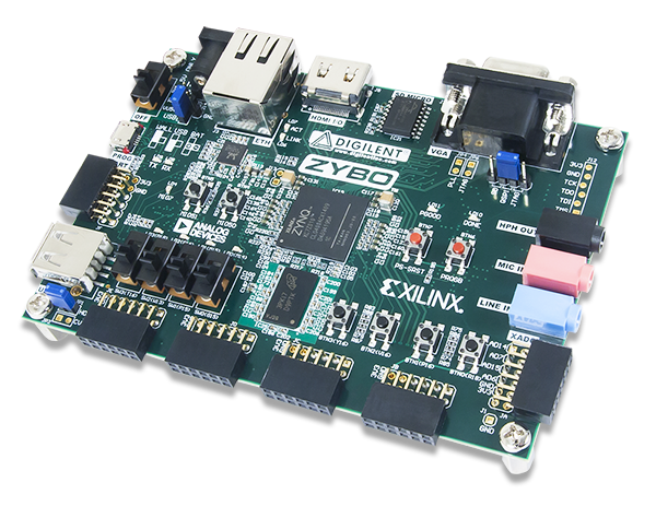
- Set address in SD card.
- Set command code 2.
- Write data to a buffer located in programmable logic.
- Run the command.
- Wait until the command completes.
- Reset team completion status.
Implemented Test:for (SectorAddress = 0; SectorAddress < 1048576; SectorAddress ++)
{
if ((SectorAddress % 1024) == 0)
{
xil_printf("Data write to %d sector \n\r", SectorAddress);
}
Xil_Out32(0x43c00008, SectorAddress);
Xil_Out32(0x43c00004, 2);
for (int32_t i = 0; i < 1024; i++)
{
Xil_Out32(0x43c00014, cntrData);
cntrData++;
}
Xil_Out32(0x43c00000, 1);
for (;;)
{
status = Xil_In32(0x43c0000c);
if (status == 0x01 || status == 0x03)
{
if (status == 0x03)
{
xil_printf("Error in write \n\r");
}
break;
}
else
{
cntrDuration++;
usleep(100);
}
}
durationWrite += cntrDuration;
if (cntrDuration > MaxWrite )
{
MaxWrite = cntrDuration;
}
cntrDuration = 0x00;
Xil_Out32(0x43c00000, 0);
SectorAddress += 7;
}
To the question of why the outer boundary of 1024 is used in the cycle. The number of blocks is set to 8. The size of one block is 512 bytes. The total size of 8 data blocks is 8 * 512 bytes = 4096 bytes. The bus between the processor module and the programmable logic is 4 bytes in size. It turns out that to send 4096 bytes of 4 bytes from the processor module to the programmable logic, it is necessary to perform 4096/4 = 1024 write operations.When working on the processor module, the data reading algorithm will be as follows:- Set address in SD card.
- Set command code 1.
- Run the command.
- Wait until the command completes.
- Reset team completion status.
- Read data from the buffer in programmable logic.
Implemented Test:for (SectorAddress = 0; SectorAddress < 1048576; SectorAddress++)
{
if ((SectorAddress % 1024) == 0)
{
xil_printf("Data read from %d sector \n\r", SectorAddress);
}
Xil_Out32(0x43c00008, SectorAddress);
Xil_Out32(0x43c00004, 1);
Xil_Out32(0x43c00000, 1);
for (;;)
{
status = Xil_In32(0x43c0000c);
if (status == 0x01 || status == 0x03)
{
if (status == 0x03)
{
xil_printf("Error in read \n\r");
}
break;
}
else
{
cntrDuration++;
usleep(100);
}
}
durationRead += cntrDuration;
if (cntrDuration > MaxRead )
{
MaxRead = cntrDuration;
}
cntrDuration = 0x00;
Xil_Out32(0x43c00000, 0);
for (int32_t i = 0; i < 1024; i++)
{
DataR = Xil_In32(0x43c0001c);
if (DataR != cntrData)
{
xil_printf("Data corrupt! \n\r");
}
DataR = Xil_In32(0x43c00020);
cntrData++;
}
SectorAddress += 7;
}
When working on the processor module, the data erasure algorithm will be as follows:- Set address in SD card.
- Set command code 4.
- Run the command.
- Wait until the command completes.
- Reset team completion status.
Implemented Test:for (SectorAddress = 0; SectorAddress < 1048576; SectorAddress++)
{
if ((SectorAddress % 1024) == 0)
{
xil_printf("Data erase from %d sector \n\r", SectorAddress);
}
Xil_Out32(0x43c00008, SectorAddress);
Xil_Out32(0x43c00004, 4);
Xil_Out32(0x43c00000, 1);
for (;;)
{
status = Xil_In32(0x43c0000c);
if (status == 0x01 || status == 0x03)
{
if (status == 0x03)
{
xil_printf("Error in write! \n\r");
}
break;
}
else
{
cntrDuration++;
usleep(100);
}
}
durationErase += cntrDuration;
if (cntrDuration > MaxErase )
{
MaxErase = cntrDuration;
}
cntrDuration = 0x00;
Xil_Out32(0x43c00000, 0);
SectorAddress += 7;
}
Test completely on github.4. Results
A 16 GB card was used. During testing, 2 GB of data was recorded, 2 GB of data was read, and 2 GB of data was erased.The conclusions are disappointing. When using FPGA, it makes no sense to use the SD card in SPI mode, except for the case when it is very necessary to store large amounts of data without presenting speed requirements.