In this part, we will consider which way the information about the pressed key from the keyboard to the CPU goes, there will be a lot of pictures and this is not the last part. I will talk about this from the point of view of a programmer who writes in user mode - user programs, web, mobile applications - therefore, there may be inaccuracies. People involved in electronics are unlikely to find anything useful for themselves. The first part is here .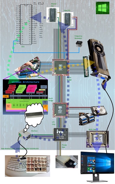
for (int i = 0; i < COLSC; i++) {
 	SetPower(columns[i], 3.0 f);
  	for (int j = 0; j < ROWSC; j++) {
    		float power = GetPower(rows[j]);
    		if (power >= 3.0f - THRESHOLD) {
      			BYTE key = keys[i, j];
      			SendKey(key);
    		}
  	}
}
Each key corresponds to a scan code, it is standardized and is an 8-bit number, i.e. one byte. Therefore, when the Y key is pressed, the keyboard controller will have to send the number 21 (0x15), and when released - 149 (0x95). How is the shipment done? Surely you worked with JSON, web services or sent data between processes and you know that to send data you need to serialize , i.e. turn into an array of bytes or formatted text that the recipient can deserialize , i.e. recreate an object in its address space. And what can serialize data at such a low level? We need to transfer only 1 byte (8 bits). Looking ahead, I’ll say that we will transmit data bit by bit.In mathematics, there is a formula that can convert any decimal number that is familiar to us into a sequence of zeros and ones and vice versa. This formula has found application in computer technology. In the first part, I casually mentioned that analog technology exploits the laws of physics, while digital works at the level of zeros and ones. This means that an analog telephone encodes the entire spectrum of the human voice into a sequence of electromagnetic waves, and a digital telephone uses a chip that converts the human voice into digital data, for example, in WAV files, and then transmits them in a sequence of zeros and ones in the form of electromagnetic waves. Only in this case, instead of the entire spectrum of the voice, only two values must be represented - 0 and 1. They can be represented by waves of different lengths, different voltages,light pulses through the optical fiber, black and white stripes on paper, holes on the punch card.The scan code of the pressed Y key in binary looks like 0001 0101. We will transmit them along the microcontroller leg which is responsible for the data ( DATA ). Logical unit is 3.3V or higher, logical zero- voltage is about 0V. Here's the catch - how do I pass three zeros in a row? To do this, we need a second leg which we will call CLOCK, when on it one means that the transmission session of one bit has begun, and zero has ended. Such a change in the values (voltages) will occur with a certain time interval, say 50 nanoseconds, because at the other end there is a second microcontroller that works at its own speed and listens to the legs to which CLOCK and DATA are connected in an endless loop. In this example, I will assume that the keyboard is connected via the PS2 connector, which is shown below. Through the USB port, the transfer algorithm will be different. As you can see, the PS2 port has pins called Data, Clock.In addition to them, there is also a contact through which the PS2 port controller distributes the 5V voltage necessary for operation to the keyboard and a ground contact, which is simply displayed on the keyboard body. Other contacts are not used.The PS / 2 port is called a serial bus , because it transmits bits one by one (a sequence of bits). The parallel port transfers data through several contacts at once and can transfer for example one byte (8 bits) at once for one data transfer session.What is the difference between a port, a bus, and a protocol? A bus, like a port, is a set of contacts (wiring) and an agreement on how to use them, only the port has a connection for connecting external devices, and the bus is used to communicate components on the motherboard. A port is essentially a bus with a connector in the middle. A protocol is an interaction through contacts. In the example with PS / 2, this was the order of data transfer through the Clock and Data contacts.
Previously, the Intel 8042 microcontroller was very common and was used both in the keyboard and as a PS2 port controller, i.e. two identical chips exchanged data. The PS2 port driver in Windows is called 8042prt.sys.
In fact, we transmit not 8 bits, but 11, because the data is transmitted as a data packet or message . An additional 3 bits indicate the beginning and end of the data - one zero at the beginning and 0 1 at the end, such a protocol for transferring data from the device to the host in PS2. This may look like the SendKey function in pseudo-code, if you prefer to understand the code. It sends data about the pressed key via the PS2 bus.
void SendBit(BYTE bit) {
	float power = (bit != 0) ? 3.3f : 0.0f;
	SetPower(DATA, power);
	SetPower(CLOCK, 3.3f);
	Sleep(50);
	SetPower(CLOCK, 0.0f);
	Sleep(50);
}

void SendData(BYTE data) {
	SendBit(0);

	for (BYTE i = 0; i < sizeof(BYTE); i++) {
		BYTE bit = (data >> i) & 1;
		SendBit(bit);
	}

	SendBit(0);
	SendBit(1);
}
It is not always necessary to manually set the voltage on each leg individually for data transfer. In some cases, the value stored in the register is automatically displayed on the contacts.
On the graph, such a data transfer will be visualized as follows. Time is along the X axis, and voltage is along the Y axis.In analogue technology, the signal may be distorted, i.e. the wire is not connected to anything, but the voltmeter shows 0.5V on it due to the fact that there is an electromagnetic field nearby. Therefore, the concept of threshold voltage is used. If the voltage is less than the threshold, then we assume that we got a logical zero, otherwise unity. Taking into account possible distortions, the scan code of the pressed Y key can come like this:Before we take a closer look at how data from the keyboard gets to the CPU, let's talk about microchips , buses, and motherboards .Microcontrollers and microcircuits
The microcontroller can execute a program sewn into it, has a certain amount of RAM memory and a place to store data and program code. In the chip, the program can be set at the design stage. Manually creating an electrical circuit implementing an algorithm is very time-consuming and therefore, a special programming language called VHDL (Hardware Description Language) can be used to design microcircuits . This is a high-level programming language that is translated into a circuit plan, it is run through a program that finds the optimal location of the radio elements on the board and is ultimately made in physical form. Images are for illustrative purposes only.How are the data and commands represented in microchips and microcontrollers? The basis of computer technology is a transistor, which mankind has learned to make in microscopic dimensions. A transistor is such a radio element that has three legs: an input, an output, and between them a control that opens or closes a current between two legs. The figure below illustrates the operation of the transistor, water illustrates the current.Voltage is applied to the input leg, if the control has voltage, then the current passes to the output, otherwise there will be 0V. Having 8 transistors, each of which has an LED connected to the output leg that either lights up or not, we can imagine 256 unique combinations (2 to the power of 8). Lapochki are interpreted from right to left, as well as decimal numbers. The lower digits are on the right.Those. one bulb represents one bit of information (0 or 1), and eight such bulbs correspond to one byte. It is possible to build logical operators AND, OR, NOT, XOR on transistors.For example, in the AND operator circuit (on the left in the picture above), the output will only have voltage if both input voltages are non-zero. Someone already has invented algorithms for addition, multiplication, division, and subtraction based on bitwise logical operations and bit shifts. Chip manufacturers just need to implement them. The operation of the bitwise addition algorithm is illustrated below; we will not analyze it:The nanotransistors are microscopic and can be placed on the board in the millions. The Intel processor is shown below and how approximately one of its cores might look like. The picture is illustrative.Microcircuits may contain a microcontroller on the same board and in the same case.Tires
Typically, in textbooks, tires are shown as bold arrows, as in the picture below. This is done so as not to draw all the connections of the contacts, which can be many. The operation of the PS2 bus is very simple, all you need is three pins. But there are buses which, for example, have 124 contacts for data transfer.There are the following types of tires:- Data - bits on these contacts are interpreted as data: number, symbol, part of a picture or other binary data. Bus width affects throughput, number of bits transmitted per second
- Addresses - bits on these pins are interpreted as a physical address in memory. The width of this bus determines the maximum supported RAM capacity.
- — . CPU RAM I/O.
- . , . ATX 24 Pin 12V PSU Connector, .
A tire may consist of substrates , i.e. some contacts are used for data, others for addresses, others for control and contacts to which power is transmitted. The approach when the same contacts are used alternately to transmit both data and addresses is called multiplexing . For example, the Intel 8086 processor has a data and address bus of 20 bits, on the pin diagram its contacts are indicated by AD0-AD19 (legs 16-2 and 39-35).In a more complex case, we may have several microcircuits connected to the same contacts. For normal communication, they need an additional chip that will determine who at what point in time can use them, it is called a bus controller. In the figure below, a spherical bus in a vacuum: four identical microcontrollers transmit data to the consumer microcontroller via the bus controller. The red wire is the voltage that the bus controller distributes to all the chips connected to it. Data is transmitted through the green wires and “negotiating” with the bus controller is performed, and the blue wire is Clock, through which the bus controller synchronizes the communication of the controllers, because they can operate at different speeds. If the logical unit is on the blue wire, then the chip entitled to use the bus can perform one act of interaction with the outside world - read a bit, for example.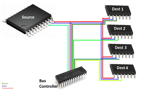
- Slow - keyboard, hard drive, network card, audio, etc.
- Fast - CPU, RAM, GPU.
Based on this division, the motherboard has two main chips - the South Bridge , which coordinates the work of all slow devices, and the North Bridge, for coordination of fast devices. In modern computers, the Northbridge is located in the CPU itself, and the Southbridge may be called the Platform Controller Hub, but this does not change the essence. Both of these bridges are interconnected by a bus through which they inform each other about significant events. Of particular interest is the clock generator by which the processor, RAM and graphics card synchronize their work, the same blue wire. Overclockingthis is essentially changing the BIOS settings so that synchronization occurs more often, while the hardware, primarily the CPU, will heat up harder, consume more power and more quickly develop its resource. The opposite is underclocking , when the speed decreases to save battery power or reduce noise.A chipset is a set of chips that were all designed to work with each other. They provide communication between components on the motherboard and provide functionality such as timers. The chip set works with only one processor brand, AMD cannot be inserted into the motherboard with the Intel chipset, they even have different contacts. The motherboard diagram is presented below:Want an example of hardware encapsulation? Intel chipsets have a chip called Super IO , it is shown in the picture below and is connected to the South Bridge via the LPC bus. LPC is the smart name for wiring CLOCK, DATA, VCC (POWER). This chip contains the emulation of all the old chips that have ever been used for peripherals, including the 8042 chip that was used for the PS2 port. There is also a port controller emulator for Floppy and other relics that interfere with progress. In the general diagram of the motherboard, both Super IO and the LPC bus are indicated above .The modern PS2 port connects directly to the Super I / O chip. Green is the keyboard, purple is the mouse. Previously, it connected to the Intel 8042 microcontroller.The motherboard is made of dielectric, i.e. material that does not conduct current. The current can pass only about the lines printed on the board. The motherboard has many layers, each of which has its own contacts printed and therefore if you drill the motherboard where the lines are not visible, you can spoil it by damaging the invisible contacts inside the board. Now you can take a closer look at the process of distributing data from the PS2 to the CPU.The road from the PS2 to the processor
Typically, computer architecture is considered on the 8086 processor. On the one hand, this is correct, because it is quite simple compared to modern CPUs, and on the other hand, it is wrong, because it is old and does not reflect the architecture of a modern machine. Intel 8086 did not need any bridges, because it was so slow that it could work with peripherals on one bus, i.e. at one frequency. I don’t know the modern CPU and chip sets, so I will explain it on fictitious ones that resemble real ones. In my example, there will be a fictional CPU very similar to Intel 8086. The Super IO chip has more than one hundred contacts and there is documentation on the Internet, but I don’t see the point of sorting out which pins the keyboard and LPC bus actually use to communicate with South Bridge. The main thing is the principle, which can be implemented in different ways.Let's take a quick look at the picture to remember that we have already passed. The green arrows indicate the path we will take.So, the data from the keyboard has already come to the PS2 port controller, which was once an Intel 8042 chip, and is now emulated by a Super IO chip. And now let's analyze the further course of actions on my fictional motherboard with a fictional CPU. The PS2 controller received a scan code of the pressed Y key and now supplies voltage to the contact signal (purple line, see the picture below) on which the programmable interrupt controller should notify about data from the keyboard. This signal is transmitted from one chip to another until the North Bridge passes it to the interrupt manager.Programmable Interrupt Controller is an Intel 8259 chip in which 8 legs (their names IRQ0-IRQ7) are reserved for receiving notifications from certain ports ( I nterrupt R e Q uest). A keyboard is tied to IRQ1 pin, IRQ7 to a printer, Floppy disk to some pin, sound card, parallel ports and others . Of course, there can be much more than eight devices, so a technique such as cascading was used when another similar PIC was connected to a leg with the name IRQ2, at which the count did not start from 0, but 7. The mouse is tied to IRQ12, i.e. foot IRQ5 on the second PIC.The interrupt controller should now notify the CPU of the event on the keyboard. This happens as follows:- INT (Interrupt) , INTR (Interrupt Request) . CPU , , .. . , . exception .
- INTR, .
- ( D0-D7) , . PIC ( IRQ).
, ? . . — (x, y, z, w). . - CPU AD0-AD7 , . IDT (Interrupt Descriptior Table) , , . CPU .
. . , IDT C# .
struct IDT_entry{
	unsigned short int offset_lowerbits;
	unsigned short int selector;
	unsigned char zero;
	unsigned char type_attr;
	unsigned short int offset_higherbits;
};

struct IDT_entry IDT[256];
- , INTA (Interrupt Acknowledged).
The keyboard interrupt handler in the simplest code will look like this. It calls a command that signals the completion of interrupt processing, i.e. sends a signal to the INTA foot.void irq1_handler(void) {
outb(0x20, 0x20);
}
You can learn more about how the interrupt vector table is configured on osdev .Now we know how the interrupt happened, but we don’t know how the interrupt handler reads information about the pressed key. From a software point of view, the PS2 port is two registers, only they are not accessed by names or addresses in memory by the I / O port number . These two single-byte registers are assigned to ports 0x60 and 0x64, the first (0x60) will contain the scan code of the key. The second port is used to transfer status and commands to the PS2 port (not the keyboard!). The x86 architecture instruction set has the command IN storeTo , fromPortNumwhich reads the value from the specified I / O port into the specified register. For example IN AL, 0x60 will save the data from the keyboard to the AL register. It might work something like this:- In the processor that we are considering there are legs AD0-AD20, they can be used to indicate the address and data. This is both a data bus and an address bus. In addition to them, there are a number of control legs, for example, pin No. 28 (S2), the value of which will indicate to the north bridge where the reading will take place - from memory or an input / output device. The IN command sets the value here talking about the I / O device.
- CPU (- AD0-AD20) 0110 0000, 0x60. CPU , . , - , - . 0x60 SuperIO , - .
- Super IO . 0x60 PS2, .
- . Intel 8042, SuperIO, LPC , . .. , .
- CPU (- 8 AD0-AD20).
- CPU AL. .
This whole algorithm works on a nanosecond scale and therefore runs almost instantly, even though the processor spent some time waiting for the I / O operation.As you now understand reading from external devices, even such as RAM memory with so on. CPU is rather slow. This slowness can be noticed by writing a program that prints 10,000 lines in a file line by line, instead of copying them to the buffer and saving immediately. The hard drive is connected to the South Bridge and inside it there is also a controller that controls the direct placement of data.RAM is connected to the CPU via the bus and reading from it takes some time. To speed up the CPU, it has a cache, i.e. The area in which transistors are located representing data that will soon be needed or often used, their reading is much faster than from the RAM board, which communicates with the CPU through the North Bridge. RAM is called Dynamic Random Access Memory , because capacitors are used to represent data in it. A capacitor is a radio element that, like a battery, holds a charge for a while until it is completely discharged. Only here discharge occurs very quickly. Therefore, the capacitors must be recharged, this happens instantly, it is enough to apply voltage. Charged capacitor - logical 1, otherwise 0. For cache memory is usedStatic RAM i.e. it does not need to be recharged and therefore it works faster, but costs more. The cache is divided into 3 levels, which are sequentially checked during the search for the requested data before the processor accesses the RAM. On older processors, the first level cache (L1) was part of the CPU and worked with it at the same frequency, when both L2 and L3 caches were external chips. Now they are all on the same chip with the processor. L1 cache is the fastest and smallest in memory size, L2 has more memory but slower. L3 is the largest cache and the slowest, often called the shared cache , because it stores data for all CPU cores, while L1 and L2 are created for each individual core.In the next part, we will talk about how Windows receives and processes the received data.